参数资料
| 型号: | AD8651ARM-R2 |
| 厂商: | Analog Devices Inc |
| 文件页数: | 7/20页 |
| 文件大小: | 0K |
| 描述: | IC OPAMP VF CMOS 50MHZ LN 8MSOP |
| 标准包装: | 1 |
| 系列: | DigiTrim® |
| 放大器类型: | 电压反馈 |
| 电路数: | 1 |
| 输出类型: | 满摆幅 |
| 转换速率: | 41 V/µs |
| 增益带宽积: | 50MHz |
| 电流 - 输入偏压: | 1pA |
| 电压 - 输入偏移: | 100µV |
| 电流 - 电源: | 9.5mA |
| 电流 - 输出 / 通道: | 40mA |
| 电压 - 电源,单路/双路(±): | 2.7 V ~ 5.5 V,±1.35 V ~ 2.75 V |
| 工作温度: | -40°C ~ 125°C |
| 安装类型: | 表面贴装 |
| 封装/外壳: | 8-TSSOP,8-MSOP(0.118",3.00mm 宽) |
| 供应商设备封装: | 8-MSOP |
| 包装: | 标准包装 |
| 其它名称: | AD8651ARM-R2DKR |
Data Sheet
AD8651/AD8652
Rev. D | Page 15 of 20
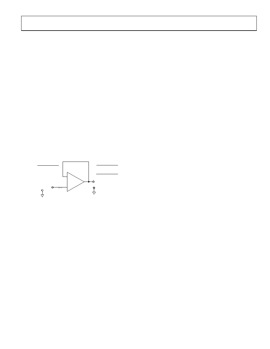
Input Protection
As with any semiconductor device, if a condition exists for the
input voltage to exceed the power supply, the device input
overvoltage characteristic must be considered. The inputs of the
AD865x family are protected with ESD diodes to either power
supply. Excess input voltage energizes internal PN junctions in
the AD865x, allowing current to flow from the input to the
supplies. This results in an input stage with picoamps of input
current that can withstand up to 4000 V ESD events (human
body model) with no degradation.
Excessive power dissipation through the protection devices
destroys or degrades the performance of any amplifier. Differential
voltages greater than 7 V result in an input current of approximately
(| VCC – VEE | – 0.7 V)/RI, where RI is the resistance in series with
the inputs. For input voltages beyond the positive supply, the
input current is approximately (VIN – VCC – 0.7)/RI. For input
voltages beyond the negative supply, the input current is about
(VIN – VEE + 0.7)/RI. If the inputs of the amplifier sustain
differential voltages greater than 7 V or input voltages beyond
the amplifier power supply, limit the input current to 10 mA by
using an appropriately sized input resistor (RI), as shown in
(| VCC – VEE | – 0.7V)
30mA
FOR LARGE | VCC – VEE |
FOR VIN BEYOND
SUPPLY VOLTAGES
RI >
RI
– VIN +
+ VO
30mA
(VIN – VEE + 0.7V)
RI >
30mA
(VIN – VEE – 0.7V)
RI >
+
–
AD865x
03301-
054
Figure 55. Input Protection Method
Overdrive Recovery
Overdrive recovery is defined as the time it takes for the output
of an amplifier to come off the supply rail after an overload signal is
initiated. This is usually tested by placing the amplifier in a closed-
loop gain of 15 with an input square wave of 200 mV p-p while the
amplifier is powered from either 5 V or 3 V. The AD865x family
has excellent recovery time from overload conditions (see Figure 31
and Figure 32). The output recovers from the positive supply rail
within 200 ns at all supply voltages. Recovery from the negative rail
is within 100 ns at 5 V supply.
LAYOUT, GROUNDING, AND BYPASSING
CONSIDERATIONS
Power Supply Bypassing
Power supply pins can act as inputs for noise, so care must be
taken that a noise-free, stable dc voltage is applied. The purpose
of bypass capacitors is to create low impedances from the supply
to ground at all frequencies, thereby shunting or filtering most
of the noise.
Bypassing schemes are designed to minimize the supply
impedance at all frequencies with a parallel combination of
capacitors of 0.1 F and 4.7 F. Chip capacitors of 0.1 F (X7R
or NPO) are critical and should be as close as possible to the
amplifier package. The 4.7 F tantalum capacitor is less critical
for high frequency bypassing, and, in most cases, only one is
needed per board at the supply inputs.
Grounding
A ground plane layer is important for densely packed PC
boards to spread the current-minimizing parasitic inductances.
However, an understanding of where the current flows in a
circuit is critical to implementing effective high speed circuit
design. The length of the current path is directly proportional to
the magnitude of parasitic inductances and, therefore, the high
frequency impedance of the path. High speed currents in an
inductive ground return create an unwanted voltage noise.
The length of the high frequency bypass capacitor leads is
critical. A parasitic inductance in the bypass grounding works
against the low impedance created by the bypass capacitor.
Place the ground leads of the bypass capacitors at the same
physical location. Because load currents also flow from the
supplies, the ground for the load impedance should be at the
same physical location as the bypass capacitor grounds. For the
larger value capacitors, intended to be effective at lower
frequencies, the current return path distance is less critical.
Leakage Currents
Poor PC board layout, contaminants, and the board insulator
material can create leakage currents that are much larger than the
input bias current of the AD865x family. Any voltage differential
between the inputs and nearby traces sets up leakage currents
through the PC board insulator, for example 1 V/100 G = 10 pA.
Similarly, any contaminants on the board can create significant
leakage (skin oils are a common problem).
To significantly reduce leakages, put a guard ring (shield)
around the inputs and the input leads that are driven to the
same voltage potential as the inputs. This ensures that there is
no voltage potential between the inputs and the surrounding
area to set up any leakage currents. To be effective, the guard
ring must be driven by a relatively low impedance source and
should completely surround the input leads on all sides, above
and below, using a multilayer board.
Another effect that can cause leakage currents is the charge
absorption of the insulator material itself. Minimizing the
amount of material between the input leads and the guard
ring helps to reduce the absorption. Also, low absorption
materials, such as Teflon or ceramic, may be necessary in
some instances.
相关PDF资料 |
PDF描述 |
|---|---|
| TSW-137-23-L-D | CONN HEADER 74POS .100" DL GOLD |
| SMF8.5AT1G | TVS ZENER 200W 8.5V SOD123FL |
| 0034.3111.PT | FUSE 250MA 250V 5X20 T-LAG GLASS |
| RGH1608-2C-P-162-B | RES 1.6K OHM 1/6W 0.1% 0603 SMD |
| TSW-138-23-L-D | CONN HEADER 76POS .100" DL GOLD |
相关代理商/技术参数 |
参数描述 |
|---|---|
| AD8651ARM-REEL | 制造商:Analog Devices 功能描述:OP Amp Single GP R-R I/O 5.5V 8-Pin MSOP T/R 制造商:Rochester Electronics LLC 功能描述:SINGLE, PRECISION CMOS RAIL-RAIL OP AMP - Tape and Reel |
| AD8651ARMZ | 功能描述:IC OPAMP VF CMOS 50MHZ LN 8MSOP RoHS:是 类别:集成电路 (IC) >> Linear - Amplifiers - Instrumentation 系列:DigiTrim® 标准包装:50 系列:- 放大器类型:通用 电路数:2 输出类型:满摆幅 转换速率:1.8 V/µs 增益带宽积:6.5MHz -3db带宽:4.5MHz 电流 - 输入偏压:5nA 电压 - 输入偏移:100µV 电流 - 电源:65µA 电流 - 输出 / 通道:35mA 电压 - 电源,单路/双路(±):1.8 V ~ 5.25 V,±0.9 V ~ 2.625 V 工作温度:-40°C ~ 85°C 安装类型:表面贴装 封装/外壳:10-TFSOP,10-MSOP(0.118",3.00mm 宽) 供应商设备封装:10-MSOP 包装:管件 |
| AD8651ARMZ-R2 | 功能描述:IC OPAMP VF CMOS 50MHZ LN 8MSOP RoHS:是 类别:集成电路 (IC) >> Linear - Amplifiers - Instrumentation 系列:DigiTrim® 标准包装:2,500 系列:- 放大器类型:通用 电路数:1 输出类型:满摆幅 转换速率:0.11 V/µs 增益带宽积:350kHz -3db带宽:- 电流 - 输入偏压:4nA 电压 - 输入偏移:20µV 电流 - 电源:260µA 电流 - 输出 / 通道:20mA 电压 - 电源,单路/双路(±):2.7 V ~ 36 V,±1.35 V ~ 18 V 工作温度:-40°C ~ 85°C 安装类型:表面贴装 封装/外壳:8-SOIC(0.154",3.90mm 宽) 供应商设备封装:8-SO 包装:带卷 (TR) |
| AD8651ARMZ-R21 | 制造商:AD 制造商全称:Analog Devices 功能描述:50 MHz, Precision, Low Distortion, Low Noise CMOS Amplifiers |
| AD8651ARMZ-REEL | 功能描述:IC OPAMP VF CMOS 50MHZ LN 8MSOP RoHS:是 类别:集成电路 (IC) >> Linear - Amplifiers - Instrumentation 系列:DigiTrim® 产品培训模块:Differential Circuit Design Techniques for Communication Applications 标准包装:1 系列:- 放大器类型:RF/IF 差分 电路数:1 输出类型:差分 转换速率:9800 V/µs 增益带宽积:- -3db带宽:2.9GHz 电流 - 输入偏压:3µA 电压 - 输入偏移:- 电流 - 电源:40mA 电流 - 输出 / 通道:- 电压 - 电源,单路/双路(±):3 V ~ 3.6 V 工作温度:-40°C ~ 85°C 安装类型:表面贴装 封装/外壳:16-VQFN 裸露焊盘,CSP 供应商设备封装:16-LFCSP-VQ 包装:剪切带 (CT) 产品目录页面:551 (CN2011-ZH PDF) 其它名称:ADL5561ACPZ-R7CT |
发布紧急采购,3分钟左右您将得到回复。