- 您现在的位置:买卖IC网 > PDF目录5289 > AD8672ARZ-REEL7 (Analog Devices Inc)IC OPAMP GP 10MHZ DUAL LN 8SOIC PDF资料下载
参数资料
| 型号: | AD8672ARZ-REEL7 |
| 厂商: | Analog Devices Inc |
| 文件页数: | 5/20页 |
| 文件大小: | 0K |
| 描述: | IC OPAMP GP 10MHZ DUAL LN 8SOIC |
| 设计资源: | Sample-and-Hold Circuit Using ADG1211 Switch (CN0058) |
| 标准包装: | 1,000 |
| 放大器类型: | 通用 |
| 电路数: | 2 |
| 转换速率: | 4 V/µs |
| 增益带宽积: | 10MHz |
| 电流 - 输入偏压: | 3nA |
| 电压 - 输入偏移: | 20µV |
| 电流 - 电源: | 3mA |
| 电流 - 输出 / 通道: | 20mA |
| 电压 - 电源,单路/双路(±): | 10 V ~ 36 V,±5 V ~ 18 V |
| 工作温度: | -40°C ~ 125°C |
| 安装类型: | 表面贴装 |
| 封装/外壳: | 8-SOIC(0.154",3.90mm 宽) |
| 供应商设备封装: | 8-SO |
| 包装: | 带卷 (TR) |
Data Sheet
AD8671/AD8672/AD8674
Rev. F | Page 13 of 20
TOTAL HARMONIC DISTORTION (THD) AND NOISE
The AD8671/AD8672/AD8674 exhibit low total harmonic
distortion (THD) over the entire audio frequency range. This
makes them suitable for applications with high closed-loop
gains, including audio applications. Figure 33 shows
approximately 0.0006% of THD + N in a positive unity gain, the
worst-case configuration for distortion.
Hz
100
1k
10k
PERCENTAGE
LT1007
0.0001
0.0002
0.0005
0.0010
0.0020
0.0050
0.0100
0.0200
0.0500
0.1000
50
20
500
200
5k
2k
AD8671
20k
03718-B-035
VS = ±5V
VIN = 2.5V
RL = 600
Figure 33. Total Harmonic Distortion and Noise
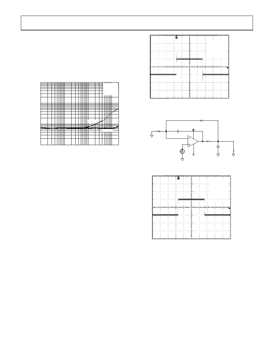
DRIVING CAPACITIVE LOADS
The AD8671/AD8672/AD8674 can drive large capacitive loads
without causing instability. However, when configured in unity
gain, driving very large loads can cause unwanted ringing or
instability.
Figure 34 shows the output of the AD8671 with a capacitive
load of 1 nF. If heavier loads are used in low closed-loop gain or
unity-gain configurations, it is recommended to use external
compensation as shown in the circuit in Figure 35. This
technique reduces the overshoot and prevents the op amp from
oscillation. The trade-off of this circuit is a reduction in output
swing. However, a great added benefit stems from the fact that
the input signal and the op amp’s noise are filtered, and thus the
overall output noise is kept to a minimum.
The output response of the circuit is shown in Figure 36.
03718-B-036
VSY = ±15V
RL = 2k
CL = 1nF
VIN = 100mV
AV = +1
CH2 +OVER
39.80%
CH2 –OVER
39.80%
TIME (10
s/DIV)
V
O
L
T
AG
E
(
500mV
/DI
V
)
Figure 34. AD8671 Capacitive Load Drive
500
RF
VCC
220pF
CF
VIN
VEE
RG
500
10
RS
1nF
CL
03718-B-037
2k
RL
Figure 35. Recommended Capacitive Load Circuit
03718-B-038
VSY = ±15V
RL = 2k
CL = 1nF
CF = 220pF
VIN = 100mV
AV = +2
CH2 +OVER
5.051%
CH2 –OVER
6.061%
TIME (10
s/DIV)
V
O
L
T
AG
E
(
100mV
/DI
V
)
Figure 36. Compensated Load Drive
相关PDF资料 |
PDF描述 |
|---|---|
| TA35-CKDWF100C0 | CIRCUIT BRKR THERMAL 10A 3POLE |
| TA35-CKDWF120C0 | CIRC BREAKER/WHITE ROCKER 3P 12A |
| LPPB022NFSS-RC | CONN HEADER .050" 4PS DL SMD AU |
| TA35-CKDWF080C0 | CIRC BREAKER/WHITE ROCKER 3P 8A |
| TA35-CKDWF070C0 | CIRC BREAKER/WHITE ROCKER 3P 7A |
相关代理商/技术参数 |
参数描述 |
|---|---|
| AD8672TRZ-EP | 功能描述:IC OPAMP GP 10MHZ 8SOIC 制造商:analog devices inc. 系列:- 零件状态:在售 放大器类型:通用 电路数:2 输出类型:- 压摆率:4 V/μs 增益带宽积:10MHz 电流 - 输入偏置:3nA 电压 - 输入失调:20μV 电流 - 电源:3mA 电流 - 输出/通道:30mA 电压 - 电源,单/双(±):±5 V ~ 15 V 工作温度:-55°C ~ 125°C 标准包装:98 |
| AD8672TRZ-EP-R7 | 功能描述:IC OPAMP GP 10MHZ 8SOIC 制造商:analog devices inc. 系列:- 零件状态:Digi-Key 停止供應 放大器类型:通用 电路数:2 输出类型:- 压摆率:4 V/μs 增益带宽积:10MHz 电流 - 输入偏置:3nA 电压 - 输入失调:20μV 电流 - 电源:3mA 电流 - 输出/通道:30mA 电压 - 电源,单/双(±):±5 V ~ 15 V 工作温度:-55°C ~ 125°C 标准包装:1 |
| AD8674 | 制造商:AD 制造商全称:Analog Devices 功能描述:Precision, Very Low Noise, Low Input Bias Current Operational Amplifiers |
| AD8674AR | 制造商:Analog Devices 功能描述:OP Amp Quad GP 制造商:Analog Devices 功能描述:OP AMP QUAD LOW NOISE SMD 8674 |
| AD8674AR-REEL | 制造商:Analog Devices 功能描述:OP Amp Quad GP 制造商:Analog Devices 功能描述:OP Amp Quad GP ±15V 14-Pin SOIC N T/R |
发布紧急采购,3分钟左右您将得到回复。