参数资料
| 型号: | AD8801ARZ |
| 厂商: | Analog Devices Inc |
| 文件页数: | 12/16页 |
| 文件大小: | 0K |
| 描述: | IC DAC 8BIT OCTAL W/SD 16-SOIC |
| 产品培训模块: | Data Converter Fundamentals DAC Architectures |
| 标准包装: | 48 |
| 系列: | TrimDAC® |
| 设置时间: | 600ns |
| 位数: | 8 |
| 数据接口: | 串行 |
| 转换器数目: | 8 |
| 电压电源: | 单电源 |
| 功率耗散(最大): | 27.5mW |
| 工作温度: | -40°C ~ 85°C |
| 安装类型: | 表面贴装 |
| 封装/外壳: | 16-SOIC(0.154",3.90mm 宽) |
| 供应商设备封装: | 16-SOIC |
| 包装: | 管件 |
| 输出数目和类型: | 8 电压,单极 |
| 采样率(每秒): | 1.7M |
| 产品目录页面: | 785 (CN2011-ZH PDF) |
AD8801/AD8803
REV. A
–5–
For example, when VREFH = +5 V and VREFL = 0 V the follow-
ing output voltages will be generated for the following codes:
DVOX
Output State
(VREFH = +5 V, VREFL = 0 V)
255
4.98 V
Full-Scale
128
2.50 V
Half-Scale (Midscale Reset Value)
1
0.02 V
1 LSB
0
0.00 V
Zero-Scale
REFERENCE INPUTS (VREFH, VREFL)
The reference input pins set the output voltage range of all eight
DACs. In the case of the AD8801 only the VREFH pin is avail-
able to establish a user designed full-scale output voltage. The
external reference voltage can be any value between 0 and VDD
but must not exceed the VDD supply voltage. In the case of the
AD8803, which has access to the VREFL which establishes the
zero-scale output voltage, any voltage can be applied between
0 V and VDD. VREFL can be smaller or larger in voltage than
VREFH since the DAC design uses fully bidirectional switches as
shown in Figure 3. The input resistance to the DAC has a code
dependent variation that has a nominal worst case measured at
55H, which is approximately 2 k. When VREFH is greater than
VREFL, the REFL reference must be able to sink current out of
the DAC ladder, while the REFH reference is sourcing current
into the DAC ladder. The DAC design minimizes reference
glitch current maintaining minimum interference between DAC
channels during code changes.
DAC OUTPUTS (O1–O8)
The eight DAC outputs present a constant output resistance of
approximately 5 k
independent of code setting. The distribu-
tion of ROUT from DAC to DAC typically matches within
±1%.
However, device to device matching is process lot dependent
having a
±20% variation. The change in R
OUT with temperature
has a 500 ppm/
°C temperature coefficient. During power shut-
down all eight outputs are open circuited.
DAC
REG
#1
EN
ADDR
DEC
DAC
REG
#8
D10
D9
D8
D7
SER
REG
D
D0
..
.
..
.
..
.
DAC
1
AD8801/AD8803
D7
D0
DAC
8
D7
D0
8
R
VDD
VREFH
O1
O2
O3
O4
O5
O6
O7
O8
CS
CLK
SDI
SHDN
GND
RS
VREFL
.
..
.
..
(AD8801 ONLY)
(AD8803 ONLY)
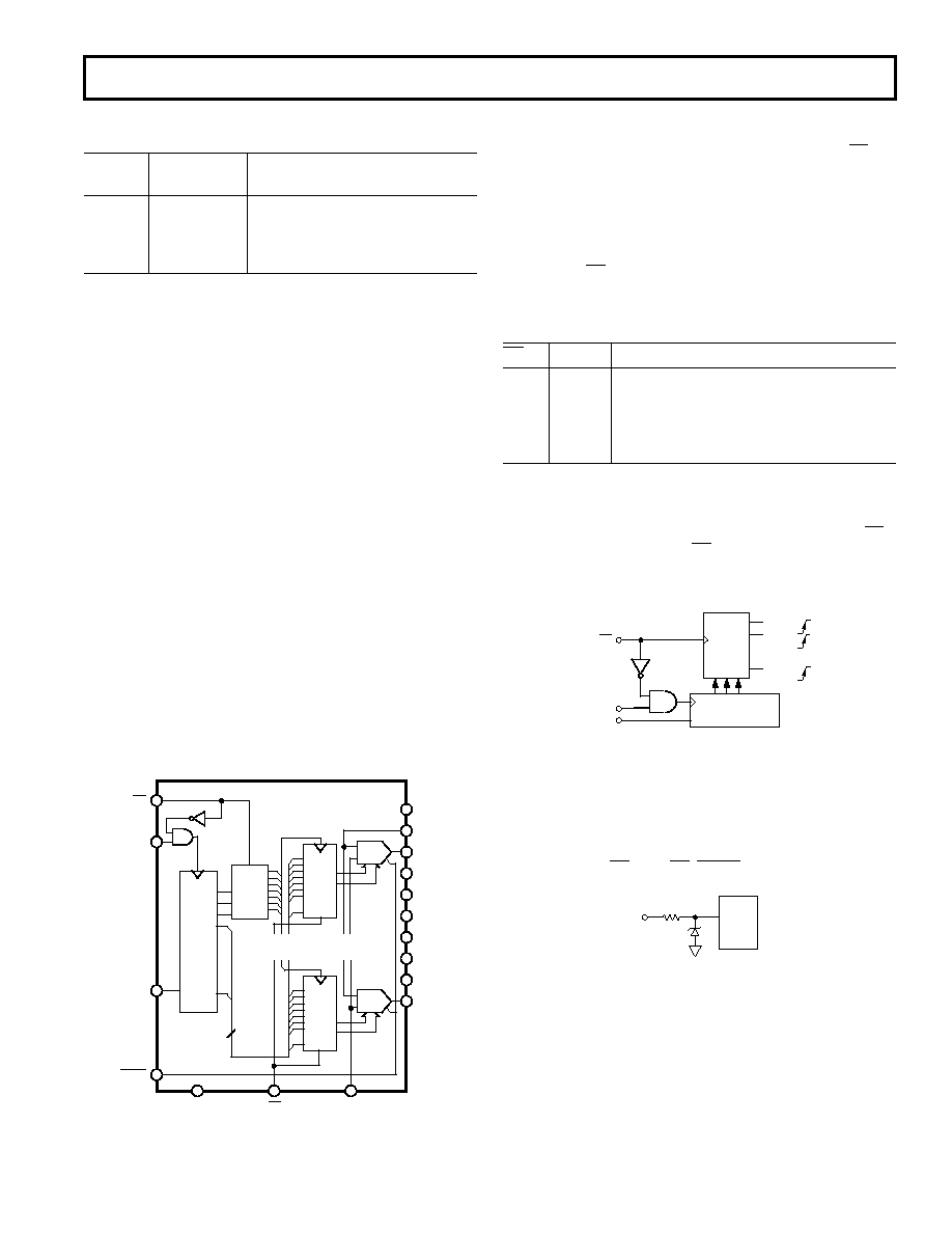
Figure 4. Block Diagram
DIGITAL INTERFACING
The AD8801/AD8803 contains a standard three-wire serial in-
put control interface. The three inputs are clock (CLK), CS and
serial data input (SDI). The positive-edge sensitive CLK input
requires clean transitions to avoid clocking incorrect data into
the serial input register. Standard logic families work well. If
mechanical switches are used for product evaluation, they
should be debounced by a flip-flop or other suitable means. Fig-
ure 4 block diagram shows more detail of the internal digital cir-
cuitry. When CS is taken active low, the clock can load data into
the serial register on each positive clock edge, see Table II.
Table II.
Input Logic Control Truth Table
CS
CLK
Register Activity
1
X
No effect.
0
P
Shifts Serial Register one bit loading the
next bit in from the SDI pin.
P
X
Data is transferred from the serial register
to the decoded DAC register. See Figure 5.
NOTE: P = positive edge, X = don’t care.
The data setup and data hold times in the specification table
determine the data valid time requirements. The last 11 bits of
the data word entered into the serial register are held when CS
returns high. At the same time CS goes high it gates the address
decoder which enables one of the eight positive edge triggered
DAC registers, see Figure 5 detail.
...
DAC 1
DAC 2
DAC 8
ADDR
DECODE
SERIAL
REGISTER
CS
CLK
SDI
Figure 5. Equivalent Control Logic
The target DAC register is loaded with the last eight bits of the se-
rial data word completing one DAC update. Eight separate 11-bit
data words must be clocked in to change all eight output settings.
All digital inputs are protected with a series input resistor and
parallel Zener ESD structure shown in Figure 6. This applies to
digital input pins CS, SDI, RS, SHDN, CLK.
LOGIC
100
Figure 6. Equivalent ESD Protection Circuit
Digital inputs can be driven by voltages exceeding the AD8801/
AD8803 VDD value. This allows 5 V logic to interface directly to
the part when it is operated at 3 V.
相关PDF资料 |
PDF描述 |
|---|---|
| SY100EPT22VZG | IC TRANSLATOR DIFF 3.3V 8-SOIC |
| ICS84330AV-02LFT | IC SYNTHESIZER 700MHZ 28-PLCC |
| SY10ELT22ZG | IC TRANSLATOR PECL TTL DFF 8SOIC |
| MS3454W14S-7S | CONN RCPT 3POS JAM NUT W/SCKT |
| SY10ELT21ZG | IC TRANSLATOR 3.3V DIFF 8-SOIC |
相关代理商/技术参数 |
参数描述 |
|---|---|
| AD8801ARZ-REEL | 功能描述:IC DAC 8BIT OCTAL W/SD 16SOIC RoHS:是 类别:集成电路 (IC) >> 数据采集 - 数模转换器 系列:TrimDAC® 产品培训模块:LTC263x 12-, 10-, and 8-Bit VOUT DAC Family 特色产品:LTC2636 - Octal 12-/10-/8-Bit SPI VOUT DACs with 10ppm/°C Reference 标准包装:91 系列:- 设置时间:4µs 位数:10 数据接口:MICROWIRE?,串行,SPI? 转换器数目:8 电压电源:单电源 功率耗散(最大):2.7mW 工作温度:-40°C ~ 85°C 安装类型:表面贴装 封装/外壳:14-WFDFN 裸露焊盘 供应商设备封装:14-DFN-EP(4x3) 包装:管件 输出数目和类型:8 电压,单极 采样率(每秒):* |
| AD8802 | 制造商:AD 制造商全称:Analog Devices 功能描述:12 Channel, 8-Bit TrimDACs with Power Shutdown |
| AD8802AN | 制造商:Analog Devices 功能描述:DAC 12-CH R-2R 8-bit 20-Pin PDIP N Tube 制造商:Analog Devices 功能描述:SEMICONDUCTORSLINEAR |
| AD8802ANZ | 功能描述:IC DAC 8BIT 12CH W/SD 20DIP RoHS:是 类别:集成电路 (IC) >> 数据采集 - 数模转换器 系列:TrimDAC® 标准包装:2,400 系列:- 设置时间:- 位数:18 数据接口:串行 转换器数目:3 电压电源:模拟和数字 功率耗散(最大):- 工作温度:-40°C ~ 85°C 安装类型:表面贴装 封装/外壳:36-TFBGA 供应商设备封装:36-TFBGA 包装:带卷 (TR) 输出数目和类型:* 采样率(每秒):* |
| AD8802AR | 功能描述:IC DAC 8BIT 12CH W/SD 20-SOIC RoHS:否 类别:集成电路 (IC) >> 数据采集 - 数模转换器 系列:TrimDAC® 标准包装:47 系列:- 设置时间:2µs 位数:14 数据接口:并联 转换器数目:1 电压电源:单电源 功率耗散(最大):55µW 工作温度:-40°C ~ 85°C 安装类型:表面贴装 封装/外壳:28-SSOP(0.209",5.30mm 宽) 供应商设备封装:28-SSOP 包装:管件 输出数目和类型:1 电流,单极;1 电流,双极 采样率(每秒):* |
发布紧急采购,3分钟左右您将得到回复。