参数资料
| 型号: | AD8803AR |
| 厂商: | Analog Devices Inc |
| 文件页数: | 10/16页 |
| 文件大小: | 0K |
| 描述: | IC DAC 8BIT OCTAL W/SD 16-SOIC |
| 产品培训模块: | Data Converter Fundamentals DAC Architectures |
| 标准包装: | 48 |
| 系列: | TrimDAC® |
| 设置时间: | 600ns |
| 位数: | 8 |
| 数据接口: | 串行 |
| 转换器数目: | 8 |
| 电压电源: | 单电源 |
| 功率耗散(最大): | 27.5mW |
| 工作温度: | -40°C ~ 85°C |
| 安装类型: | 表面贴装 |
| 封装/外壳: | 16-SOIC(0.154",3.90mm 宽) |
| 供应商设备封装: | 16-SOIC |
| 包装: | 管件 |
| 输出数目和类型: | 8 电压,单极 |
| 采样率(每秒): | 1.7M |
AD8801/AD8803
REV. A
–3–
ORDERING GUIDE
Package
Model
FTN
Temperature
Description
Option
AD8801AN
RS
–40
°C to +85°C PDIP-16
N-16
AD8801AR
RS
–40
°C to +85°C SO-16
R-16A
AD8803AN
REFL
–40
°C to +85°C PDIP-16
N-16
AD8803AR
REFL
–40
°C to +85°C SO-16
R-16A
AD8803 PIN DESCRIPTIONS
Pin Name
Description
1VREFH
Common High-Side DAC Reference Input
2
O1
DAC Output #1, Addr = 0002
3
O2
DAC Output #2, Addr = 0012
4
O3
DAC Output #3, Addr = 0102
5
O4
DAC Output #4, Addr = 0112
6
SHDN
Reference inputs open circuit, active low, all
DAC outputs open circuit. DAC latch settings
maintained.
7
CS
Chip Select Input, active low. When CS returns
high, data in the serial input register is decoded
based on the address bits and loaded into the tar-
get DAC register.
8
GND
Ground
9VREFL
Common Low-Side DAC Reference Input
10
CLK
Serial Clock Input, Positive Edge Triggered
11
SDI
Serial Data Input
12
O5
DAC Output #5, Addr = 1002
13
O6
DAC Output #6, Addr = 1012
14
O7
DAC Output #7, Addr = 1102
15
O8
DAC Output #8, Addr = 1112
16
VDD
Positive power supply, specified for operation at
both +3 V and +5 V.
ABSOLUTE MAXIMUM RATINGS
(TA = +25°C, unless otherwise noted)
VDD to GND . . . . . . . . . . . . . . . . . . . . . . . . . . . . . . –0.3, +8 V
VREFX to GND . . . . . . . . . . . . . . . . . . . . . . . . . . . . . . 0 V, VDD
Outputs (Ox) to GND . . . . . . . . . . . . . . . . . . . . . . . . 0 V, VDD
Digital Input Voltage to GND . . . . . . . . . . . . . . . . . . 0 V, VDD
Operating Temperature Range . . . . . . . . . . . . . –40
°C to +85°C
Maximum Junction Temperature (TJ MAX) . . . . . . . . +150°C
Storage Temperature . . . . . . . . . . . . . . . . . . . –65
°C to +150°C
Lead Temperature (Soldering, 10 sec) . . . . . . . . . . . . . +300
°C
Package Power Dissipation . . . . . . . . . . . . . (TJ MAX – TA)/θJA
Thermal Resistance
θ
JA,
SOIC (SO-16) . . . . . . . . . . . . . . . . . . . . . . . . . . . . . 60
°C/W
P-DIP (N-16) . . . . . . . . . . . . . . . . . . . . . . . . . . . . . . 57
°C/W
AD8801 PIN DESCRIPTIONS
Pin Name
Description
1VREFH
Common DAC Reference Input
2
O1
DAC Output #1, Addr = 0002
3
O2
DAC Output #2, Addr = 0012
4
O3
DAC Output #3, Addr = 0102
5
O4
DAC Output #4, Addr = 0112
6
SHDN
Reference input open circuit, active low, all
DAC outputs open circuit. DAC latch settings
maintained.
7
CS
Chip Select Input, active low. When CS returns
high, data in the serial input register is decoded
based on the address bits and loaded into the tar-
get DAC register.
8
GND
Ground
9
CLK
Serial Clock Input, Positive Edge Triggered
10
SDI
Serial Data Input
11
O5
DAC Output #5, Addr = 1002
12
O6
DAC Output #6, Addr = 1012
13
O7
DAC Output #7, Addr = 1102
14
O8
DAC Output #8, Addr = 1112
15
RS
Asynchronous preset to midscale output setting,
active low. Loads all DAC latches with 80H.
16
VDD
Positive power supply, specified for operation at
both +3 V and +5 V.
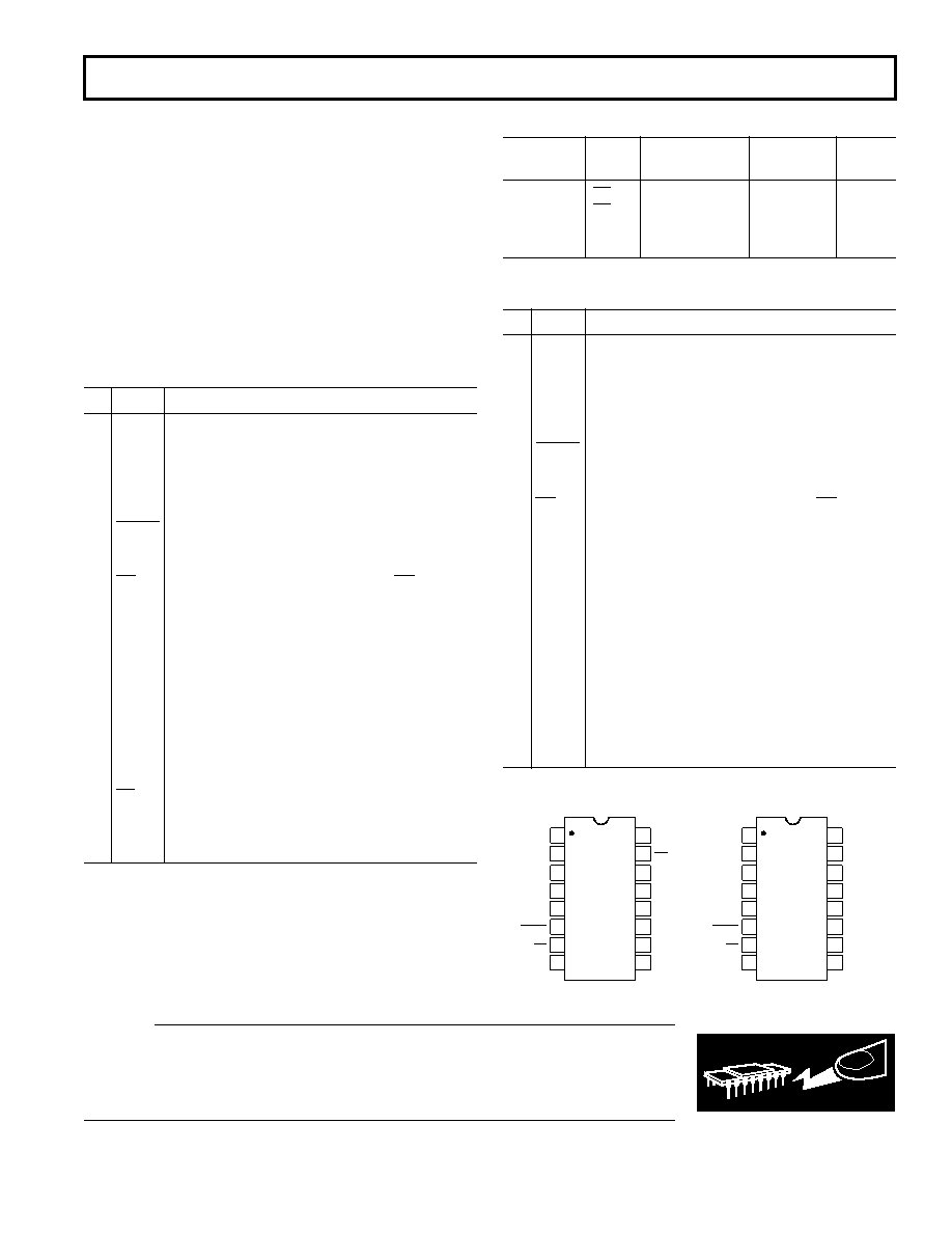
PIN CONFIGURATIONS
VREFH
O1
VDD
RS
O4
SHDN
CS
O6
O5
SDI
O2
O3
O8
O7
GND
CLK
1
2
16
15
5
6
7
12
11
10
3
4
14
13
89
TOP VIEW
(Not to Scale)
AD8801
VREFH
O1
VDD
O8
O4
SHDN
CS
O5
SDI
CLK
O2
O3
O7
O6
GND
VREFL
1
2
16
15
5
6
7
12
11
10
3
4
14
13
89
TOP VIEW
(Not to Scale)
AD8803
WARNING!
ESD SENSITIVE DEVICE
CAUTION
ESD (electrostatic discharge) sensitive device. Electrostatic charges as high as 4000 V readily
accumulate on the human body and test equipment and can discharge without detection.
Although these devices feature proprietary ESD protection circuitry, permanent damage may
occur on devices subjected to high energy electrostatic discharges. Therefore, proper ESD
precautions are recommended to avoid performance degradation or loss of functionality.
相关PDF资料 |
PDF描述 |
|---|---|
| AD9042ASTZ | IC ADC 12BIT 41MSPS 44-TQFP |
| AD9051BRSRL-2V | IC ADC 10BIT 60MSPS 28-SSOP |
| AD9054ABSTZ-200 | IC ADC 8BIT 200MSPS 44-LQFP |
| AD9057BRS-RL40 | IC ADC 8BIT 40MSPS 20-SSOP T/R |
| AD9058AKD | IC ADC 8BIT DUAL 50MSPS 48-CDIP |
相关代理商/技术参数 |
参数描述 |
|---|---|
| AD8803AR-REEL | 制造商:Analog Devices 功能描述:DAC 8-CH R-2R 8-bit 16-Pin SOIC N T/R 制造商:Rochester Electronics LLC 功能描述:8CH 8-BIT TRIMDAC W/PWR SHDN - Tape and Reel |
| AD8803ARZ | 功能描述:IC DAC 8BIT OCTAL W/SD 16-SOIC RoHS:是 类别:集成电路 (IC) >> 数据采集 - 数模转换器 系列:TrimDAC® 产品培训模块:Lead (SnPb) Finish for COTS Obsolescence Mitigation Program 标准包装:50 系列:- 设置时间:4µs 位数:12 数据接口:串行 转换器数目:2 电压电源:单电源 功率耗散(最大):- 工作温度:-40°C ~ 85°C 安装类型:表面贴装 封装/外壳:8-TSSOP,8-MSOP(0.118",3.00mm 宽) 供应商设备封装:8-uMAX 包装:管件 输出数目和类型:2 电压,单极 采样率(每秒):* 产品目录页面:1398 (CN2011-ZH PDF) |
| AD8803ARZ | 制造商:Analog Devices 功能描述:IC 8-BIT TDAC |
| AD8803ARZ-REEL | 功能描述:IC DAC 8BIT OCTAL W/SD 16SOIC RoHS:是 类别:集成电路 (IC) >> 数据采集 - 数模转换器 系列:TrimDAC® 产品培训模块:LTC263x 12-, 10-, and 8-Bit VOUT DAC Family 特色产品:LTC2636 - Octal 12-/10-/8-Bit SPI VOUT DACs with 10ppm/°C Reference 标准包装:91 系列:- 设置时间:4µs 位数:10 数据接口:MICROWIRE?,串行,SPI? 转换器数目:8 电压电源:单电源 功率耗散(最大):2.7mW 工作温度:-40°C ~ 85°C 安装类型:表面贴装 封装/外壳:14-WFDFN 裸露焊盘 供应商设备封装:14-DFN-EP(4x3) 包装:管件 输出数目和类型:8 电压,单极 采样率(每秒):* |
| AD8804 | 制造商:AD 制造商全称:Analog Devices 功能描述:12 Channel, 8-Bit TrimDACs with Power Shutdown |
发布紧急采购,3分钟左右您将得到回复。