参数资料
| 型号: | AD8803ARZ |
| 厂商: | Analog Devices Inc |
| 文件页数: | 16/16页 |
| 文件大小: | 0K |
| 描述: | IC DAC 8BIT OCTAL W/SD 16-SOIC |
| 产品培训模块: | Data Converter Fundamentals DAC Architectures |
| 标准包装: | 48 |
| 系列: | TrimDAC® |
| 设置时间: | 600ns |
| 位数: | 8 |
| 数据接口: | 串行 |
| 转换器数目: | 8 |
| 电压电源: | 单电源 |
| 功率耗散(最大): | 27.5mW |
| 工作温度: | -40°C ~ 85°C |
| 安装类型: | 表面贴装 |
| 封装/外壳: | 16-SOIC(0.154",3.90mm 宽) |
| 供应商设备封装: | 16-SOIC |
| 包装: | 管件 |
| 输出数目和类型: | 8 电压,单极 |
| 采样率(每秒): | 1.7M |
| 产品目录页面: | 785 (CN2011-ZH PDF) |
AD8801/AD8803
REV. A
–9–
VH
VL
VH
VL
VH
VL
VREFH VDD
+5V
GND
VREFL
DIGITAL INTERFACING
OMITTED FOR CLARITY
R1
100k
OP291
AD8801/
AD8803
SIMPLE BUFFER
0V TO 5V
SUMMER CIRCUIT
WITH FINE TRIM
ADJUSTMENT
Figure 23. Buffering the AD8801/AD8803 Output
Increasing Output Voltage Swing
An external amplifier can also be used to extend the output volt-
age swing beyond the power supply rails of the AD8801/AD8803.
This technique permits an easy digital interface for the DAC,
while expanding the output swing to take advantage of higher
voltage external power supplies. For example, DAC A of Fig-
ure 24 is configured to swing from –5 V to +5 V. The actual
output voltage is given by:
VOUT = 1 +
R
F
RS
×
D
256
× 5V
()–5V
Where D is the DAC input value (i.e., 0 to 255). This circuit
can be combined with the “fine/coarse” circuit of Figure 23 if,
for example, a very accurate adjustment around 0 V is desired.
A
VDD
VREFH
GND
VREFL
AD8801/
AD8803
B
+5V
+12V
–5V
OP191
OP193
RF
100k
RS
100k
–5V TO +4.98V
0V TO +10V
100k
100k
+5V
Figure 24. Increasing Output Voltage Swing
DAC B of Figure 24 is in a noninverting gain of two configura-
tion, which increases the available output swing to +10 V. The
feedback resistors can be adjusted to provide any scaling of the
output voltage, within the limits of the external op amp power
supplies.
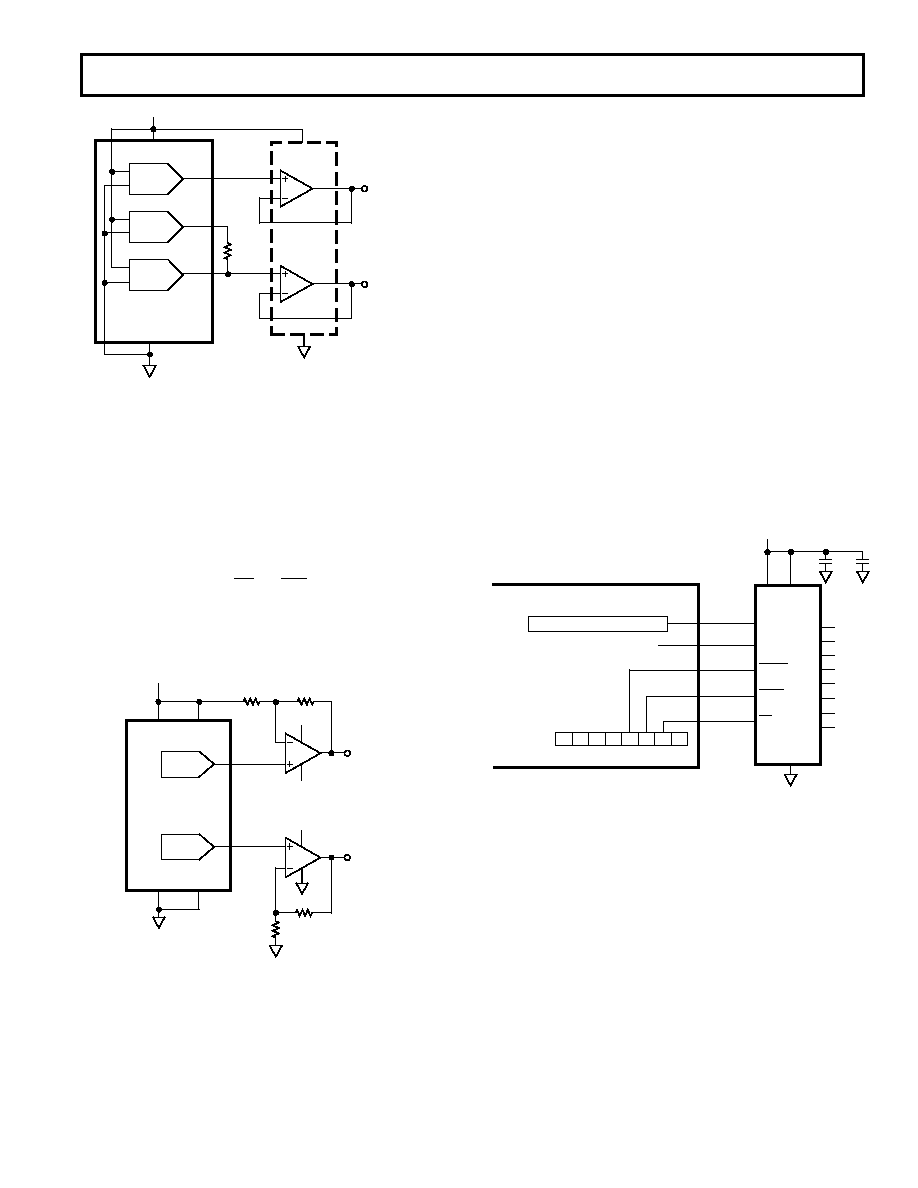
Microcomputer Interfaces
The AD8801/AD8803 serial data input provides an easy inter-
face to a variety of single-chip microcomputers (
Cs). Many Cs
have a built-in serial data capability that can be used for com-
municating with the DAC. In cases where no serial port is pro-
vided, or it is being used for some other purpose (such as an
RS-232 communications interface), the AD8801/AD8803 can
easily be addressed in software.
Eleven data bits are required to load a value into the AD8801/
AD8803 (3 bits for the DAC address and 8 bits for the DAC
value). If more than 11 bits are transmitted before the Chip Se-
lect input goes high, the extra (i.e., the most-significant) bits are
ignored. This feature is valuable because most
Cs only transmit
data in 8-bit increments. Thus, the
C will send 16 bits to the
DAC instead of 11 bits. The AD8801/AD8803 will only re-
spond to the last 11 bits clocked into the SDI input, however, so
the serial data interface is not affected.
An 8051
C Interface
A typical interface between the AD8801/AD8803 and an 8051
C is shown in Figure 25. This interface uses the 8051’s internal
serial port. The serial port is programmed for Mode 0 opera-
tion, which functions as a simple 8-bit shift register. The 8051’s
Port3.0 pin functions as the serial data output, while Port3.1
serves as the serial clock.
O1
O2
O3
O4
O5
O6
O7
O8
SDI
SCLK
RESET
SHDN
CS
VDD VREFH
GND
AD8801
+5V
P3.0
P3.1
P1.3
P1.2
P1.1
SERIAL DATA SHIFT REGISTER
RxD
TxD
SHIFT CLOCK
1.1
1.2
1.3
PORT 1
SBUF
8051 C
0.1F
10F
+
Figure 25. Interfacing the 8051
C to an AD8801/AD8803,
Using the Serial Port
When data is written to the Serial Buffer Register (SBUF, at
Special Function Register location 99H), the data is automati-
cally converted to serial format and clocked out via Port3.0 and
Port3.1. After 8 bits have been transmitted, the Transmit Inter-
rupt flag (SCON.1) is set and the next 8 bits can be transmitted.
The AD8801 and AD8803 require the Chip Select to go low at
the beginning of the serial data transfer. In addition, the SCLK
input must be high when the Chip Select input goes high at the
end of the transfer. The 8051’s serial clock meets this require-
ment, since Port3.1 both begins and ends the serial data in the
high state.
Software for the 8051 Interface
A software routine for the AD8801/AD8803 to 8051 interface is
shown in Listing 1. The routine transfers the 8-bit data stored at
data memory location DAC_VALUE to the AD8801/AD8803
DAC addressed by the contents of location DAC_ADDR.
相关PDF资料 |
PDF描述 |
|---|---|
| SY100EPT21LKG | IC TRANSLATOR DIFF 3.3V 8-MSOP |
| M83723/96G14076 | CONN PLUG 7POS STRAIGHT W/PINS |
| AD8801ARZ | IC DAC 8BIT OCTAL W/SD 16-SOIC |
| SY100EPT22VZG | IC TRANSLATOR DIFF 3.3V 8-SOIC |
| ICS84330AV-02LFT | IC SYNTHESIZER 700MHZ 28-PLCC |
相关代理商/技术参数 |
参数描述 |
|---|---|
| AD8803ARZ | 制造商:Analog Devices 功能描述:IC 8-BIT TDAC |
| AD8803ARZ-REEL | 功能描述:IC DAC 8BIT OCTAL W/SD 16SOIC RoHS:是 类别:集成电路 (IC) >> 数据采集 - 数模转换器 系列:TrimDAC® 产品培训模块:LTC263x 12-, 10-, and 8-Bit VOUT DAC Family 特色产品:LTC2636 - Octal 12-/10-/8-Bit SPI VOUT DACs with 10ppm/°C Reference 标准包装:91 系列:- 设置时间:4µs 位数:10 数据接口:MICROWIRE?,串行,SPI? 转换器数目:8 电压电源:单电源 功率耗散(最大):2.7mW 工作温度:-40°C ~ 85°C 安装类型:表面贴装 封装/外壳:14-WFDFN 裸露焊盘 供应商设备封装:14-DFN-EP(4x3) 包装:管件 输出数目和类型:8 电压,单极 采样率(每秒):* |
| AD8804 | 制造商:AD 制造商全称:Analog Devices 功能描述:12 Channel, 8-Bit TrimDACs with Power Shutdown |
| AD8804AN | 制造商:Analog Devices 功能描述:DAC 12-CH R-2R 8-bit 20-Pin PDIP N Tube 制造商:Rochester Electronics LLC 功能描述:12CH 8BIT TDAC W/VREFL SHDWN - Bulk |
| AD8804ANZ | 功能描述:IC DAC 8BIT 12CH W/SD 20DIP RoHS:是 类别:集成电路 (IC) >> 数据采集 - 数模转换器 系列:TrimDAC® 标准包装:1 系列:- 设置时间:4.5µs 位数:12 数据接口:串行,SPI? 转换器数目:1 电压电源:单电源 功率耗散(最大):- 工作温度:-40°C ~ 125°C 安装类型:表面贴装 封装/外壳:8-SOIC(0.154",3.90mm 宽) 供应商设备封装:8-SOICN 包装:剪切带 (CT) 输出数目和类型:1 电压,单极;1 电压,双极 采样率(每秒):* 其它名称:MCP4921T-E/SNCTMCP4921T-E/SNRCTMCP4921T-E/SNRCT-ND |
发布紧急采购,3分钟左右您将得到回复。