- 您现在的位置:买卖IC网 > PDF目录373958 > AD9057BRS-40 (ANALOG DEVICES INC) 8-Bit 40 MSPS/50 MSPS/80 MSPS Converter PDF资料下载
参数资料
| 型号: | AD9057BRS-40 |
| 厂商: | ANALOG DEVICES INC |
| 元件分类: | ADC |
| 英文描述: | 8-Bit 40 MSPS/50 MSPS/80 MSPS Converter |
| 中文描述: | 1-CH 8-BIT FLASH METHOD ADC, PARALLEL ACCESS, PDSO20 |
| 封装: | MO-150AE, SSOP-20 |
| 文件页数: | 8/12页 |
| 文件大小: | 184K |
| 代理商: | AD9057BRS-40 |
AD9057
–8–
REV. B
T he AD9057 provides high impedance digital output operation
when the ADC is driven into power-down mode (PWRDN,
logic HIGH). A 200 ns (minimum) power-down time should be
provided before a high impedance characteristic is required at
the outputs. A 200 ns power-up period should be provided to
ensure accurate ADC output data after reactivation (valid output
data is available three clock cycles after the 200 ns delay).
Timing
T he AD9057 is guaranteed to operate with conversion rates
from 5 MSPS to 80 MSPS depending on grade. T he ADC is
designed to operate with an encode duty cycle of 50%, but per-
formance is insensitive to moderate variations. Pulse width varia-
tions of up to
±
10% (allowing the encode signal to meet the
minimum/maximum HIGH/LOW specifications) will cause no
degradation in ADC performance (see Figure 1 timing diagram).
Power Dissipation
T he power dissipation of the AD9057 is specified to reflect a
typical application setup under the following conditions: analog
input is –0.5 dBFS at 10.3 MHz, V
D
is +5 V, V
DD
is +3 V, and
digital outputs are loaded with 7 pF typical (10 pF maximum).
T he actual dissipation will vary as these conditions are modified
in user applications. Figure 8 shows typical power consumption
for the AD9057 versus ADC encode frequency and V
DD
supply
voltage.
A power-down function allows users to reduce power dissipation
when ADC data is not required. A T T L/CMOS HIGH signal
(PWRDN) shuts down portions of the ADC and brings total
power dissipation to less than 10 mW. T he internal bandgap
voltage reference remains active during power-down mode to
minimize ADC reactivation time. If the power-down function is
not desired, Pin 1 should be tied to ground.
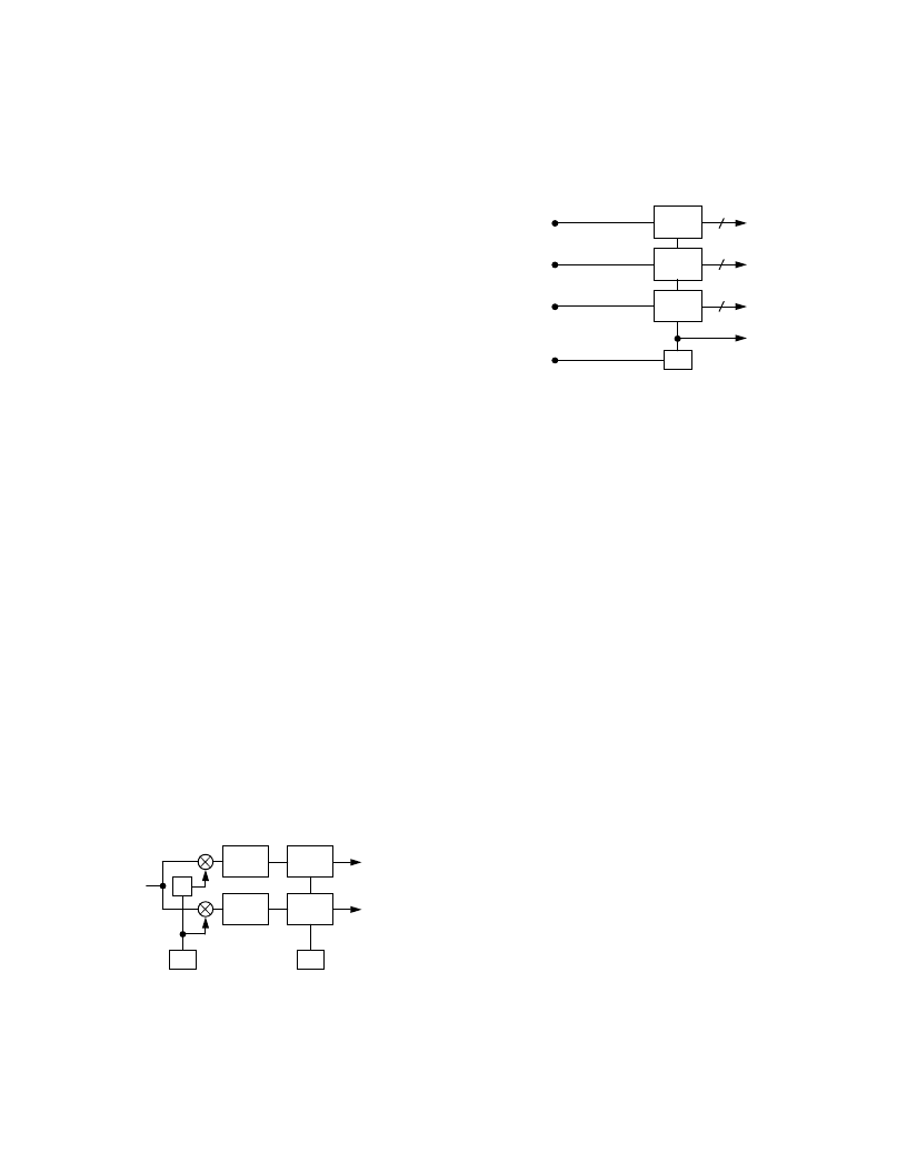
APPLIC AT IONS
T he wide analog bandwidth of the AD9057 makes it attractive
for a variety of high performance receiver and encoder applica-
tions. Figure 16 shows two ADCs in a typical low cost I & Q
demodulator implementation for cable, satellite, or wireless
LAN modem receivers. T he excellent dynamic performance of
the ADC at higher analog input frequencies and encode rates
empowers users to employ direct IF sampling techniques (refer
to Figure 3 spectral plot). IF sampling eliminates or simplifies
analog mixer and filter stages to reduce total system cost and
power.
BPF
BPF
AD9057
AD9057
VCO
90
°
VCO
IF IN
Figure 16. I & Q Digital Receiver
T he high sampling rate and analog bandwidth of the AD9057
are ideal for computer RGB video digitizer applications. With a
full-power analog bandwidth of 2
×
the maximum sampling
rate, the ADC provides sufficient pixel to pixel transient set-
tling time to ensure accurate 60 MSPS video digitization. Fig-
ure 17 shows a typical RGB video digitizer implementation for
the AD9057.
AD9057
AD9057
PLL
AD9057
PIXEL CLOCK
RED
GREEN
BLUE
H-SYNC
8
8
8
Figure 17. RGB Video Encoder
E valuation Board
T he AD9057/PCB evaluation board provides an easy to use
analog/digital interface for the 8-bit, 60 MSPS ADC. T he
board includes typical hardware configurations for a variety of
high speed digitization evaluations. On board components
include the AD9057 (in the 20-pin SSOP package), an optional
analog input buffer amplifier, a digital output latch, board
timing drivers, an analog reconstruction digital-to-analog con-
verter, and configurable jumpers for ac coupling, dc coupling,
and power-down function testing. T he board is configured at
shipment for dc coupling using the AD9057’s internal voltage
reference.
For dc coupled analog input applications, amplifier U2 is con-
figured to operate as a unity gain inverter with adjustable offset
for the analog input signal. For full-scale ADC drive the analog
input signal should be 1 V p-p into 50
(R1) referenced to
ground (0 V). T he amplifier offsets the analog signal by
+VREF (+2.5 V typical) to center the voltage for proper ADC
input drive. For dc coupled operation, connect E1 to E2 (ana-
log input to R2) and E11 to E12 (amplifier output to analog
input of AD9057) using the board jumper connectors. DC
offset of the analog input signal can be modified by adjusting
potentiometer R10.
For ac coupled analog input applications, amplifier U2 is
removed from the analog signal path. T he analog signal is
coupled into the input of the AD9057 through capacitor C2.
T he ADC pulls analog input bias current from the VREF IN
voltage through the 1 k
resistor internal to the AD9057
(BIAS OUT ). T he analog input signal to the board should be
1 V p-p into 50
(R1) for full-scale ADC drive. For ac
coupled operation, connect E1 to E3 (analog input A to C2
feedthrough capacitor) and E10 to E12 (C2 to the analog input
and internal bias resistor) using the board jumper connectors.
T he onboard reference voltage may be used to drive the ADC
or an external reference may be applied. T o use the internal
voltage reference, connect E6 to E5 (VREF OUT to VREF
IN). T o apply an external voltage reference, connect E4 to E5
(external reference from the REF banana jack to VREF IN).
T he external voltage reference should be +2.5 V
±
10%.
相关PDF资料 |
PDF描述 |
|---|---|
| AD9057BRS-60 | 8-Bit 40 MSPS/60 MSPS/80 MSPS A/D Converter |
| AD9057PCB | 8-Bit 40 MSPS/60 MSPS/80 MSPS A/D Converter |
| AD9057-PCB | 8-Bit 40 MSPS/50 MSPS/80 MSPS Converter |
| AD9057-40 | Circular Connector; MIL SPEC:MIL-C-26482, Series I, Solder; Body Material:Aluminum; Series:PT06; Number of Contacts:19; Connector Shell Size:14; Connecting Termination:Solder; Circular Shell Style:Straight Plug; Body Style:Straight |
| AD9057-60 | Circular Connector; Body Material:Aluminum; Series:PT06; No. of Contacts:19; Connector Shell Size:14; Connecting Termination:Solder; Circular Shell Style:Straight Plug; Circular Contact Gender:Pin; Insert Arrangement:14-19 |
相关代理商/技术参数 |
参数描述 |
|---|---|
| AD9057BRS-60 | 功能描述:IC ADC 8BIT 60MSPS 20-SSOP RoHS:否 类别:集成电路 (IC) >> 数据采集 - 模数转换器 系列:- 产品培训模块:Lead (SnPb) Finish for COTS Obsolescence Mitigation Program 标准包装:2,500 系列:- 位数:12 采样率(每秒):3M 数据接口:- 转换器数目:- 功率耗散(最大):- 电压电源:- 工作温度:- 安装类型:表面贴装 封装/外壳:SOT-23-6 供应商设备封装:SOT-23-6 包装:带卷 (TR) 输入数目和类型:- |
| AD9057BRS-80 | 制造商:Analog Devices 功能描述:ADC Single Flash 80Msps 8-bit Parallel 20-Pin SSOP 制造商:Rochester Electronics LLC 功能描述:8 BIT 60 MSPS ADC - Bulk 制造商:Analog Devices 功能描述:IC 8-BIT ADC |
| AD9057BRS-RL40 | 功能描述:IC ADC 8BIT 40MSPS 20-SSOP T/R RoHS:否 类别:集成电路 (IC) >> 数据采集 - 模数转换器 系列:- 产品培训模块:Lead (SnPb) Finish for COTS Obsolescence Mitigation Program 标准包装:2,500 系列:- 位数:12 采样率(每秒):3M 数据接口:- 转换器数目:- 功率耗散(最大):- 电压电源:- 工作温度:- 安装类型:表面贴装 封装/外壳:SOT-23-6 供应商设备封装:SOT-23-6 包装:带卷 (TR) 输入数目和类型:- |
| AD9057BRS-RL60 | 制造商:Analog Devices 功能描述:ADC Single Flash 60Msps 8-bit Parallel 20-Pin SSOP T/R |
| AD9057BRSRL60SP211 | 功能描述:IC ADC 8BIT 60MSPS 20-SSOP 制造商:analog devices inc. 系列:* 零件状态:上次购买时间 标准包装:1 |
发布紧急采购,3分钟左右您将得到回复。