- 您现在的位置:买卖IC网 > PDF目录10034 > AD9058AKJ (Analog Devices Inc)IC ADC 8BIT DUAL 50MSPS 44-JLCC PDF资料下载
参数资料
| 型号: | AD9058AKJ |
| 厂商: | Analog Devices Inc |
| 文件页数: | 9/11页 |
| 文件大小: | 0K |
| 描述: | IC ADC 8BIT DUAL 50MSPS 44-JLCC |
| 标准包装: | 1 |
| 位数: | 8 |
| 采样率(每秒): | 50M |
| 数据接口: | 并联 |
| 转换器数目: | 2 |
| 功率耗散(最大): | 960mW |
| 电压电源: | 模拟和数字,双 ± |
| 工作温度: | 0°C ~ 70°C |
| 安装类型: | 表面贴装 |
| 封装/外壳: | 44-LCC(J 形引线) |
| 供应商设备封装: | 44-JLCC(16.39x16.39) |
| 包装: | 管件 |
| 输入数目和类型: | 2 个单端,单极;2 个单端,双极 |
REV.
AD9058
–7–
AD9618
COMP
ENCODE
A
ENCODE
AIN A
+VS
D0A(LSB)
–VS
D0B(LSB)
D7A(MSB)
AIN B
D7B(MSB)
AD9058
(J-LEAD)
+VREF A
+VREF B
ENCODE
B
–VREF A
–VREF B
CLOCK
ANALOG
IN A
0.125V
ANALOG
IN B
0.125V
0.1 F
+5V
–5V
0.1 F
+5V
400
50
10k
5
5k
0.1 F
10pF
1k
50k
(SEE TEXT)
CLOCK
8
1N4001
4, 19, 21,
25, 27, 42
74A
CT
273
74A
CT
273
40
1
8
38
2
6
43
3
7, 20,
26, 39
28
29
30
31
32
33
34
35
18
17
16
15
14
13
12
11
5, 9, 22,
24, 37, 41
10
36
AD9618
74ACT04
0.1 F
RZ1
RZ2
–1V
1V
150
2N3906
–5V
1/2
AD708
20k
1V
2N3904
10
+5V
150
1/2
AD708
20k
AD580
1
3
0.1 F
10k
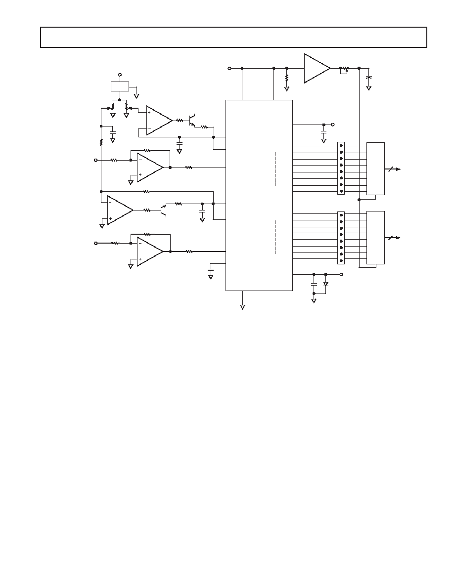
Figure 3. AD9058 Using External Voltage References
The on-board voltage reference, +VINT, is a band gap reference
that has sufficient drive capability for both reference ladders.
It provides a 2 V reference that can drive both ADCs in the
AD9058 for unipolar positive operation (0 V to 2 V).
USING THE AD9058
Refer to Figure 2. Using the internal voltage reference con-
nected to both ADCs as shown reduces the number of external
components required to create a complete data acquisition
system. The input ranges of the ADCs are positive unipolar
in this configuration, ranging from 0 V to 2 V. Bipolar input
signals are buffered, amplified, and offset into the proper input
range of the ADC using a good low distortion amplifier such
as the AD9617 or AD9618.
The AD9058 offers considerable flexibility in selecting the analog
input ranges of the ADCs; the two independent ADCs can even
have different input ranges if required. In Figure 3, the AD9058
is shown configured for
±1 V operation.
The “Reference Ladder Offset” shown in the specifications table
refers to the error between the voltage applied to the +VREF (top)
or –VREF (bottom) of the reference ladder and the voltage required
at the analog input to achieve a 1111 1111 or 0000 0000 transi-
tion. This indicates the amount of adjustment range that must be
designed into the reference circuit for the AD9058.
The diode shown between ground and –VS is normally reverse-
biased and is used to prevent latch-up. Its use is recommended
for applications in which power supply sequencing might allow
+VS to be applied before –VS; or the +VS supply is not current
limited. If the negative supply is allowed to float (the +5 V supply
is powered up before the –5 V supply), substantial +5 V supply
current will attempt to flow through the substrate (VS supply con-
tact) to ground. If this current is not limited to <500 mA, the part
may be destroyed. The diode prevents this potentially destructive
condition from occurring.
Timing
Refer to the AD9058 Timing Diagram, Figure 4. The AD9058
provides latched data outputs with no pipeline delay. To conserve
power, the data outputs have relatively slow rise and fall times.
When designing system timing, it is important to observe (1) setup
and hold times; and (2) the intervals when data is changing.
Figure 3 shows 2 k
Ω pull-down resistors on each of the D
0–D7
output data bits. When operating at conversion rates higher than
40 MSPS, these resistors help equalize rise and fall times and
ease latching the output data into external latches. The 74ACT
logic family devices have short setup and hold times and are the
recommended choices for speeds of 40 MSPS or more.
Layout
To ensure optimum performance, a single low impedance ground
plane is recommended. Analog and digital grounds should be con-
nected together and to the ground plane at the AD9058 device.
Analog and digital power supplies should be bypassed to ground
through 0.1
μF ceramic capacitors as close to the unit as possible.
For prototyping or evaluation, surface-mount sockets are available
from Methode Electronics, Inc. (Part No. 213-0320602) for
evaluating AD9058 surface-mount packages. To evaluate the
E
相关PDF资料 |
PDF描述 |
|---|---|
| SP334ET-L/TR | IC TXRX RS232/485 PROG 28WSOIC |
| IDT72V811L15TFI8 | IC FIFO SYNC 512X9 15NS 64QFP |
| MS27472T18F35S | CONN RCPT 66POS WALL MNT W/SCKT |
| LTC1321ISW#PBF | IC TXRX RS232/485/EIA562 24-SOIC |
| AD7878BQ | IC ADC 12BIT W/DSP INT 28-CDIP |
相关代理商/技术参数 |
参数描述 |
|---|---|
| AD9058ATD/883B | 功能描述:模数转换器 - ADC Dual 8-Bit 50 MSPS RoHS:否 制造商:Analog Devices 通道数量: 结构: 转换速率: 分辨率: 输入类型: 信噪比: 接口类型: 工作电源电压: 最大工作温度: 安装风格: 封装 / 箱体: |
| AD9058ATD883B | 制造商:AD 制造商全称:Analog Devices 功能描述:Dual 8-Bit 50 MSPS A/D Converter |
| AD9058ATJ | 制造商:AD 制造商全称:Analog Devices 功能描述:Dual 8-Bit 50 MSPS A/D Converter |
| AD9058ATJ/883B | 制造商:Analog Devices 功能描述:ADC Dual Flash 50Msps 8-bit Parallel 44-Pin JLCC 制造商:Analog Devices 功能描述:ADC DUAL FLASH 50MSPS 8BIT PARALLEL 44PIN JLCC - Rail/Tube 制造商:Analog Devices 功能描述:IC 8-BIT ADC |
| AD9058ATJ883B | 制造商:AD 制造商全称:Analog Devices 功能描述:Dual 8-Bit 50 MSPS A/D Converter |
发布紧急采购,3分钟左右您将得到回复。