- 您现在的位置:买卖IC网 > PDF目录17059 > AD9116-DPG2-EBZ (Analog Devices Inc)IC DAC DUAL 12BIT LO PWR 40LFCSP PDF资料下载
参数资料
| 型号: | AD9116-DPG2-EBZ |
| 厂商: | Analog Devices Inc |
| 文件页数: | 35/52页 |
| 文件大小: | 0K |
| 描述: | IC DAC DUAL 12BIT LO PWR 40LFCSP |
| 标准包装: | 1 |
| 系列: | TxDAC® |
| DAC 的数量: | 2 |
| 位数: | 12 |
| 采样率(每秒): | 125M |
| 数据接口: | 串行 |
| DAC 型: | 电流 |
| 工作温度: | -40°C ~ 85°C |
| 已供物品: | 板 |
| 已用 IC / 零件: | AD9116 |
第1页第2页第3页第4页第5页第6页第7页第8页第9页第10页第11页第12页第13页第14页第15页第16页第17页第18页第19页第20页第21页第22页第23页第24页第25页第26页第27页第28页第29页第30页第31页第32页第33页第34页当前第35页第36页第37页第38页第39页第40页第41页第42页第43页第44页第45页第46页第47页第48页第49页第50页第51页第52页
AD9114/AD9115/AD9116/AD9117
Data Sheet
Rev. C | Page 40 of 52
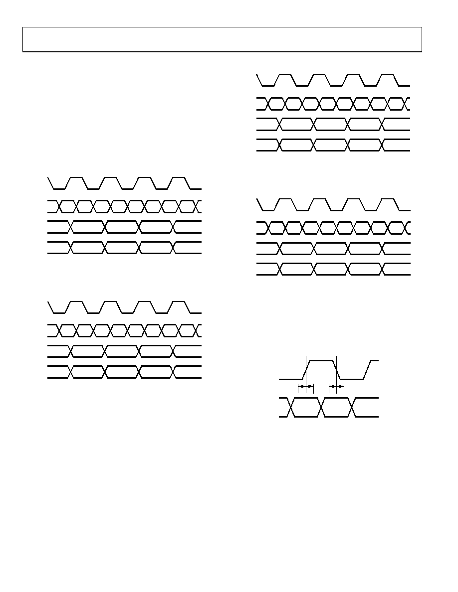
DIGITAL INTERFACE OPERATION
Digital data for the I and Q DACs is supplied over a single
parallel bus (DB[n:0], where n is 7 for the AD9114, is 9 for the
AD9115, is 11 for the AD9116, and 13 for the AD9117)
accompanied by a qualifying clock (DCLKIO). The I and Q
data are provided to the chip in an interleaved double data rate
(DDR) format. The maximum guaranteed data rate is 250 MSPS
with a 125 MHz clock. The order of data pairing and the sampling
edge selection is user programmable using the IFIRST and
IRISING data control bits, resulting in four possible timing
diagrams. These timing diagrams are shown in Figure 89,
DCLKIO
NOTES:
1. DB[n:0], WHERE n IS 7 FOR THE AD9114, 9 FOR THE AD9115, 11 FOR THE
AD9116, AND 13 FOR THE AD9117.
DB[n:0]
Z
A
B
C
D
E
F
G
H
I DATA
Z
B
D
F
Q DATA
Y
A
C
E
07466-
051
Figure 89. Timing Diagram with IFIRST = 0, IRISING = 0
DCLKIO
Z
A
B
C
D
E
F
G
H
I DATA
Y
A
C
E
Q DATA
X
Z
B
D
07466-
052
NOTES:
1. DB[n:0], WHERE n IS 7 FOR THE AD9114, 9 FOR THE AD9115, 11 FOR THE
AD9116, AND 13 FOR THE AD9117.
DB[n:0]
Figure 90. Timing Diagram with IFIRST = 0, IRISING = 1
DCLKIO
Z
A
B
C
D
E
F
G
H
I DATA
Z
B
D
F
Q DATA
A
C
E
G
07466-
053
NOTES:
1. DB[n:0], WHERE n IS 7 FOR THE AD9114, 9 FOR THE AD9115, 11 FOR THE
AD9116, AND 13 FOR THE AD9117.
DB[n:0]
Figure 91. Timing Diagram with IFIRST = 1, IRISING = 0
DCLKIO
Z
A
B
C
D
E
F
G
H
I DATA
Y
A
C
E
Q DATA
Z
B
D
F
07466-
054
NOTES:
1. DB[n:0], WHERE n IS 7 FOR THE AD9114, 9 FOR THE AD9115, 11 FOR THE
AD9116, AND 13 FOR THE AD9117.
DB[n:0]
Figure 92. Timing Diagram with IFIRST = 1, IRISING = 1
Ideally, the rising and falling edges of the clock fall in the center
of the keep-in window formed by the setup and hold times, tS
timing diagram is shown in Figure 93.
DCLKIO
DB[n:0]
tS tH
07466-
055
NOTES:
1. DB[n:0], WHERE n IS 7 FOR THE AD9114, 9 FOR THE
AD9115, 11 FOR THE AD9116, AND 13 FOR THE AD9117.
Figure 93. Setup and Hold Times for All Input Modes
In addition to the different timing modes listed in Table 2, the
input data can also be presented to the device in either unsigned
binary or twos complement format. The format type is chosen
via the TWOS data control bit.
相关PDF资料 |
PDF描述 |
|---|---|
| VE-B4X-EY | CONVERTER MOD DC/DC 5.2V 50W |
| AD9117-DPG2-EBZ | IC DAC DUAL 14BIT LO PWR 40LFCSP |
| AD9114-DPG2-EBZ | IC DAC DUAL 8BIT LO PWR 40LFCSP |
| AD9115-DPG2-EBZ | IC DAC DUAL 10BIT LO PWR 40LFCSP |
| 0210490184 | CABLE JUMPER 1.25MM .229M 12POS |
相关代理商/技术参数 |
参数描述 |
|---|---|
| AD9116-EBZ | 制造商:Analog Devices 功能描述:DUAL 12 BIT LOW POWER CONVERTER - Boxed Product (Development Kits) |
| AD9117 | 制造商:AD 制造商全称:Analog Devices 功能描述:Dual, 8-/10-/12-/14-Bit Low Power Digital-to-Analog Converters |
| AD9117BCPZ | 功能描述:IC DAC DUAL 14BIT LO PWR 40LFCSP RoHS:是 类别:集成电路 (IC) >> 数据采集 - 数模转换器 系列:TxDAC® 产品培训模块:Lead (SnPb) Finish for COTS Obsolescence Mitigation Program 标准包装:50 系列:- 设置时间:4µs 位数:12 数据接口:串行 转换器数目:2 电压电源:单电源 功率耗散(最大):- 工作温度:-40°C ~ 85°C 安装类型:表面贴装 封装/外壳:8-TSSOP,8-MSOP(0.118",3.00mm 宽) 供应商设备封装:8-uMAX 包装:管件 输出数目和类型:2 电压,单极 采样率(每秒):* 产品目录页面:1398 (CN2011-ZH PDF) |
| AD9117BCPZN | 功能描述:数模转换器- DAC Dual 14B Low Power D-A Converter RoHS:否 制造商:Texas Instruments 转换器数量:1 DAC 输出端数量:1 转换速率:2 MSPs 分辨率:16 bit 接口类型:QSPI, SPI, Serial (3-Wire, Microwire) 稳定时间:1 us 最大工作温度:+ 85 C 安装风格:SMD/SMT 封装 / 箱体:SOIC-14 封装:Tube |
| AD9117BCPZNRL7 | 功能描述:数模转换器- DAC Dual Low Pwr 14-Bit RoHS:否 制造商:Analog Devices 转换器数量:4 DAC 输出端数量:4 转换速率: 分辨率:12 bit 接口类型:Serial (I2C) 稳定时间: 最大工作温度:+ 105 C 安装风格: 封装 / 箱体:TSSOP 封装:Reel |
发布紧急采购,3分钟左右您将得到回复。