- 您现在的位置:买卖IC网 > PDF目录10664 > AD9214BRSZ-105 (Analog Devices Inc)IC ADC 10BIT 105MSPS 28-SSOP PDF资料下载
参数资料
| 型号: | AD9214BRSZ-105 |
| 厂商: | Analog Devices Inc |
| 文件页数: | 4/20页 |
| 文件大小: | 0K |
| 描述: | IC ADC 10BIT 105MSPS 28-SSOP |
| 标准包装: | 1 |
| 位数: | 10 |
| 采样率(每秒): | 105M |
| 数据接口: | 并联 |
| 转换器数目: | 1 |
| 功率耗散(最大): | 325mW |
| 电压电源: | 模拟和数字 |
| 工作温度: | -40°C ~ 85°C |
| 安装类型: | 表面贴装 |
| 封装/外壳: | 28-SSOP(0.209",5.30mm 宽) |
| 供应商设备封装: | 28-SSOP |
| 包装: | 管件 |
| 输入数目和类型: | 2 个单端,单极;1 个差分,单极 |
| 产品目录页面: | 780 (CN2011-ZH PDF) |
REV. D
AD9214
–12–
THEORY OF OPERATION
The AD9214 architecture is a bit-per-stage pipeline converter
utilizing switch capacitor techniques. These stages determine
the 7 MSBs and drive a 3-bit flash. Each stage provides suffi-
cient overlap and error correction allowing optimization of
comparator accuracy. The input buffer is differential and both
inputs are internally biased. This allows the most flexible use of
ac or dc and differential or single-ended input modes. The out-
put staging block aligns the data, carries out the error correction
and feeds the data to output buffers. The output buffers are
powered from a separate supply, allowing support of different
logic families. During power-down, the outputs go to a high
impedance state.
APPLYING THE AD9214
Encoding the AD9214
Any high-speed A/D converter is extremely sensitive to the
quality of the sampling clock provided by the user. A Track/
Hold circuit is essentially a mixer. Any noise, distortion, or
timing jitter on the clock will be combined with the desired
signal at the A/D output. For that reason, considerable care has
been taken in the design of the ENCODE input of the AD9214,
and the user is advised to give commensurate thought to the clock
source. The ENCODE input is fully TTL/CMOS compatible, and
should normally be driven directly from a low jitter, crystal-
controlled TTL/CMOS oscillator.
The ENCODE input is internally biased, allowing the user to
ac-couple in the clock signal. The cleanest clock source is often
a crystal oscillator producing a pure sine wave. Figure 7 illustrates
ac coupling such a source to the ENCODE input.
ENCODE
LOW JITTER CRYSTAL SINE OR
PULSE SOURCE 1V p-p
AD9214
Figure 7. AC-Coupled Encode Circuit
Reference Circuit
The reference circuit of the AD9214 is configured by REFSENSE
(Pin 3). By externally connecting REFSENSE to AGND, the
ADC is configured to use the internal reference (~1.25 V), and
the REF pin connection (Pin 4) is configured as an output for
the internal reference voltage.
If REFSENSE is externally connected to AVDD, the ADC is
configured to use an external reference. In this mode, the REF
pin is configured as a reference input, and must be driven by an
external 1.25 V reference.
In either configuration, the analog input voltage range (either
1 V p-p or 2 V p-p as determined by DFS/Gain) will track the
reference voltage linearly, and an external bypass capacitor should
be connected between REF and AGND to reduce noise on the
reference. In practice, no appreciable degradation in performance
occurs when an external reference is adjusted
±5%.
DFS/GAIN
The DFS/GAIN (Data Format Select/Gain) input (Pin 2)
controls both the output data format and gain (analog input volt-
age range) of the ADC. The table below describes its operation.
Table I. Data Format and Gain Configuration
External
Differential
DFS/GAIN
Analog Input
Connection
Voltage Range
Output Data Format
AGND
1 V p-p
Offset Binary
AVDD
1 V p-p
Two’s Complement
REF
2 V p-p
Two’s Complement
Floating
2 V p-p
Offset Binary
Driving the Analog Inputs
The analog input to the AD9214 is a differential buffer. As
shown in the equivalent circuits, each of the differential inputs is
internally dc biased at ~AVDD/3 to allow ac-coupling of the
analog input signal. The analog signal may be dc-coupled as
well. In this case, the dc load will be equivalent to ~10 k
to
AVDD/3, and the dc common-mode level of the analog signals
should be within the range of AVDD/3
±200 mV. For best dynamic
performance, impedances at AIN and A
IN should match.
Driving the analog input differentially optimizes ac performance,
minimizing even order harmonics and taking advantage of
common-mode rejection of noise. A differential signal may be
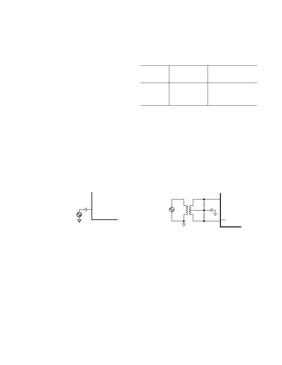
transformer-coupled, as illustrated in Figure 8, or driven from a
high-performance differential amplifier such as the AD8138
illustrated in Figure 9.
AIN
0.1 F
25
1:1
50
ANALOG
SIGNAL
SOURCE
AD9214
Figure 8. Single-Ended-to-Differential Conversion Using
a Transformer
Special care was taken in the design of the analog input section
of the AD9214 to prevent damage and corruption of data when
the input is overdriven. The optimal input range is 1.0 V p-p, but
the AD9214 can support a 2.0 V p-p input range with some degra-
dation in performance (see DFS/GAIN pin description above).
相关PDF资料 |
PDF描述 |
|---|---|
| AD7980BCPZ-RL7 | IC ADC 16BIT 1MSPS SAR 10LFCSP |
| VE-J1N-MW-F4 | CONVERTER MOD DC/DC 18.5V 100W |
| MAX9646EBS+TG45 | IC COMPARATOR W/REF 4UCSP |
| MAX3086CSD+T | IC TXRX RS485/422 10MBPS 14-SOIC |
| MAX9645EUK+T | IC COMPARATOR W/REF SOT23-5 |
相关代理商/技术参数 |
参数描述 |
|---|---|
| AD9214BRSZ-65 | 功能描述:IC ADC 10BIT 65MSPS 28SSOP RoHS:是 类别:集成电路 (IC) >> 数据采集 - 模数转换器 系列:- 其它有关文件:TSA1204 View All Specifications 标准包装:1 系列:- 位数:12 采样率(每秒):20M 数据接口:并联 转换器数目:2 功率耗散(最大):155mW 电压电源:模拟和数字 工作温度:-40°C ~ 85°C 安装类型:表面贴装 封装/外壳:48-TQFP 供应商设备封装:48-TQFP(7x7) 包装:Digi-Reel® 输入数目和类型:4 个单端,单极;2 个差分,单极 产品目录页面:1156 (CN2011-ZH PDF) 其它名称:497-5435-6 |
| AD9214BRSZ-80 | 功能描述:IC ADC 10BIT 80MSPS 28-SSOP RoHS:是 类别:集成电路 (IC) >> 数据采集 - 模数转换器 系列:- 其它有关文件:TSA1204 View All Specifications 标准包装:1 系列:- 位数:12 采样率(每秒):20M 数据接口:并联 转换器数目:2 功率耗散(最大):155mW 电压电源:模拟和数字 工作温度:-40°C ~ 85°C 安装类型:表面贴装 封装/外壳:48-TQFP 供应商设备封装:48-TQFP(7x7) 包装:Digi-Reel® 输入数目和类型:4 个单端,单极;2 个差分,单极 产品目录页面:1156 (CN2011-ZH PDF) 其它名称:497-5435-6 |
| AD9214BRSZ-RL105 | 功能描述:IC ADC 10BIT 105MSPS 28-SSOP T/R RoHS:是 类别:集成电路 (IC) >> 数据采集 - 模数转换器 系列:- 标准包装:1,000 系列:- 位数:12 采样率(每秒):300k 数据接口:并联 转换器数目:1 功率耗散(最大):75mW 电压电源:单电源 工作温度:0°C ~ 70°C 安装类型:表面贴装 封装/外壳:24-SOIC(0.295",7.50mm 宽) 供应商设备封装:24-SOIC 包装:带卷 (TR) 输入数目和类型:1 个单端,单极;1 个单端,双极 |
| AD9214BRSZ-RL65 | 功能描述:IC ADC 10BIT 65MSPS 28-SSOP T/R RoHS:是 类别:集成电路 (IC) >> 数据采集 - 模数转换器 系列:- 标准包装:1,000 系列:- 位数:16 采样率(每秒):45k 数据接口:串行 转换器数目:2 功率耗散(最大):315mW 电压电源:模拟和数字 工作温度:0°C ~ 70°C 安装类型:表面贴装 封装/外壳:28-SOIC(0.295",7.50mm 宽) 供应商设备封装:28-SOIC W 包装:带卷 (TR) 输入数目和类型:2 个单端,单极 |
| AD9214BRSZ-RL80 | 功能描述:IC ADC 10BIT 80MSPS 28-SSOP T/R RoHS:是 类别:集成电路 (IC) >> 数据采集 - 模数转换器 系列:- 标准包装:1,000 系列:- 位数:12 采样率(每秒):300k 数据接口:并联 转换器数目:1 功率耗散(最大):75mW 电压电源:单电源 工作温度:0°C ~ 70°C 安装类型:表面贴装 封装/外壳:24-SOIC(0.295",7.50mm 宽) 供应商设备封装:24-SOIC 包装:带卷 (TR) 输入数目和类型:1 个单端,单极;1 个单端,双极 |
发布紧急采购,3分钟左右您将得到回复。