- 您现在的位置:买卖IC网 > PDF目录16992 > AD9215BCP-65EBZ (Analog Devices Inc)BOARD EVAL FOR AD9215BCP-65 PDF资料下载
参数资料
| 型号: | AD9215BCP-65EBZ |
| 厂商: | Analog Devices Inc |
| 文件页数: | 6/36页 |
| 文件大小: | 0K |
| 描述: | BOARD EVAL FOR AD9215BCP-65 |
| 设计资源: | Very Low Jitter Encode (Sampling) Clocks for High Speed Analog-to-Digital Converters Using ADF4002 (CN0003) Interfacing the High Frequency AD8331 to AD9215 (CN0096) |
| 标准包装: | 1 |
| ADC 的数量: | 1 |
| 位数: | 10 |
| 采样率(每秒): | 65M |
| 数据接口: | 并联 |
| 输入范围: | 1 Vpp |
| 在以下条件下的电源(标准): | 96mW @ 65MSPS |
| 工作温度: | -40°C ~ 85°C |
| 已用 IC / 零件: | AD9215-65 |
| 已供物品: | 板 |
| 相关产品: | AD9215BRUZ-80-ND - IC ADC 10BIT 80MSPS 3V 28TSSOP AD9215BRUZ-65-ND - IC ADC 10BIT 65MSPS 3V 28TSSOP AD9215BRUZRL7-105-ND - IC ADC 10BIT 105MSPS 3V 28TSSOP AD9215BRUZRL7-65-ND - IC ADC 10BIT 65MSPS 3V 28TSSOP AD9215BRUZRL7-80-ND - IC ADC 10BIT 80MSPS 3V 28TSSOP AD9215BRUZ-105-ND - IC ADC 10BIT 105MSPS 3V 28-TSSOP AD9215BCPZ-105-ND - IC ADC 10BIT 105MSPS 3V 32-LFCSP AD9215BRU-105-ND - IC ADC 10BIT 105MSPS 3V 28-TSSOP AD9215BCPZ-80-ND - IC ADC 10BIT 80MSPS 32LFCSP AD9215BCPZ-65-ND - IC ADC 10BIT 65MSPS 32-LFCSP 更多... |
第1页第2页第3页第4页第5页当前第6页第7页第8页第9页第10页第11页第12页第13页第14页第15页第16页第17页第18页第19页第20页第21页第22页第23页第24页第25页第26页第27页第28页第29页第30页第31页第32页第33页第34页第35页第36页
AD9215
Data Sheet
Rev. B | Page 14 of 36
APPLYING THE AD9215 THEORY OF OPERATION
The AD9215 architecture consists of a front-end SHA followed
by a pipelined switched capacitor ADC. Each stage provides
sufficient overlap to correct for flash errors in the preceding
stages. The quantized outputs from each stage are combined
into a final 10-bit result in the digital correction logic. The pipe-
lined architecture permits the first stage to operate on a new
input sample, while the remaining stages operate on preceding
samples. Sampling occurs on the rising edge of the clock.
The input stage contains a differential SHA that can be config-
ured as ac-coupled or dc-coupled in differential or single-ended
modes. Each stage of the pipeline, excluding the last, consists of
a low resolution flash ADC connected to a switched capacitor
DAC and interstage residue amplifier (MDAC). The residue
amplifier magnifies the difference between the reconstructed
DAC output and the flash input for the next stage in the pipe-
line. Redundancy is used in each one of the stages to facilitate
digital correction of flash errors.
The output-staging block aligns the data, carries out the error
correction, and passes the data to the output buffers. The output
buffers are powered from a separate supply, allowing adjust-
ment of the output voltage swing. During power-down, the
output buffers go into a high impedance state.
Analog Input and Reference Overview
The analog input to the AD9215 is a differential switched
capacitor SHA that has been designed for optimum perfor-
mance while processing a differential input signal. The SHA
input can support a wide common-mode range and maintain
excellent performance, as shown in Figure 31. An input com-
mon-mode voltage of midsupply minimizes signal-dependent
errors and provides optimum performance.
02874-A-028
H
VIN+
VIN–
CPAR
T
0.5pF
T
Figure 30. Switched-Capacitor SHA Input
The clock signal alternatively switches the SHA between sample
mode and hold mode (see Figure 30). When the SHA is
switched into sample mode, the signal source must be capable
of charging the sample capacitors and settling within one-half
of a clock cycle. A small resistor in series with each input can
help reduce the peak transient current required from the output
stage of the driving source. Also, a small shunt capacitor can be
placed across the inputs to provide dynamic charging currents.
This passive network creates a low-pass filter at the ADC’s in-
put; therefore, the precise values are dependent upon the appli-
cation. In IF undersampling applications, any shunt capacitors
should be removed. In combination with the driving source
impedance, they would limit the input bandwidth.
The analog inputs of the AD9215 are not internally dc biased.
In ac-coupled applications, the user must provide this bias ex-
ternally. VCM = AVDD/2 is recommended for optimum perfor-
mance, but the device functions over a wider range with rea-
sonable performance (see Figure 31).
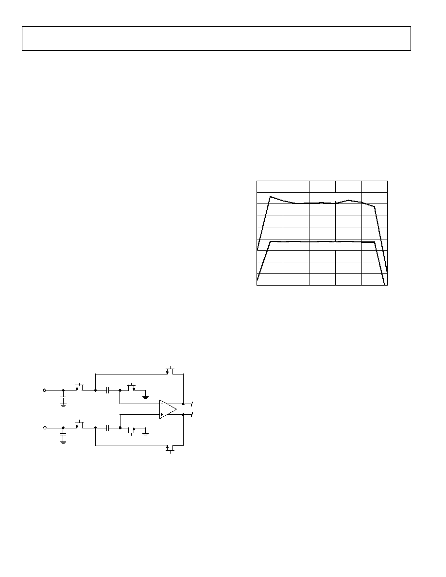
02874-A-071
40
45
50
55
60
65
70
75
80
85
0.25
0.75
1.25
1.75
2.25
2.75
dB
ANALOG INPUT COMMON-MODE VOLTAGE (V)
2V p-p SFDR
2V p-p SNR
Figure 31. AD9215-105 SNR, SFDR vs. Common-Mode Voltage
For best dynamic performance, the source impedances driving
VIN+ and VIN should be matched such that common-mode
settling errors are symmetrical. These errors are reduced by the
common-mode rejection of the ADC.
An internal differential reference buffer creates positive and
negative reference voltages, REFT and REFB, respectively, that
define the span of the ADC core. The output common mode of
the reference buffer is set to midsupply, and the REFT and
REFB voltages and span are defined as
REFT = 1/2 (AVDD + VREF)
REFB = 1/2 (AVDD VREF)
Span = 2 × (REFT REFB) = 2 × VREF
It can be seen from the equations above that the REFT and
REFB voltages are symmetrical about the midsupply voltage
and, by definition, the input span is twice the value of the VREF
voltage.
The internal voltage reference can be pin-strapped to fixed val-
ues of 0.5 V or 1.0 V or adjusted within the same range as dis-
cussed in the Internal Reference Connection section. Maximum
SNR performance is achieved with the AD9215 set to the largest
input span of 2 V p-p. The relative SNR degradation is 3 dB
相关PDF资料 |
PDF描述 |
|---|---|
| PM3316-681M-RC | INDUCTOR POWER 680UH 0.35A SMD |
| AD8332-EVALZ | BOARD EVAL FOR AD8332 |
| V2-EVAL-EXT48 | MOD V2-EVAL DAUGHTER CARD 48-PIN |
| VI-J4H-EY | CONVERTER MOD DC/DC 52V 50W |
| AD8432-EVALZ | BOARD EVALUATION FOR AD8432 |
相关代理商/技术参数 |
参数描述 |
|---|---|
| AD9215BCP-80 | 制造商:Analog Devices 功能描述:ADC Single Pipelined 80Msps 10-bit Parallel 32-Pin LFCSP EP 制造商:Rochester Electronics LLC 功能描述:10 BIT LOW POWER 65/80/105 MSPS ADC - Bulk 制造商:Analog Devices 功能描述:10BIT ADC 80MSPS 9215 LFCSP-32 |
| AD9215BCP-80EB | 制造商:Analog Devices 功能描述:Evaluation Board For AD9215 3 V A/D Converter ,10-Bit, 65/80/105 MSPS 制造商:Analog Devices 功能描述:EVAL BD FOR AD9215 3V A/D CNVRTR ,10-BIT, 65/80/105 MSPS - Bulk |
| AD9215BCP-80EBZ | 功能描述:BOARD EVAL FOR AD9215BCP-80 RoHS:是 类别:编程器,开发系统 >> 评估板 - 模数转换器 (ADC) 系列:- 产品培训模块:Obsolescence Mitigation Program 标准包装:1 系列:- ADC 的数量:1 位数:12 采样率(每秒):94.4k 数据接口:USB 输入范围:±VREF/2 在以下条件下的电源(标准):- 工作温度:-40°C ~ 85°C 已用 IC / 零件:MAX11645 已供物品:板,软件 |
| AD9215BCPZ-105 | 功能描述:IC ADC 10BIT 105MSPS 3V 32-LFCSP RoHS:是 类别:集成电路 (IC) >> 数据采集 - 模数转换器 系列:- 标准包装:1,000 系列:- 位数:12 采样率(每秒):300k 数据接口:并联 转换器数目:1 功率耗散(最大):75mW 电压电源:单电源 工作温度:0°C ~ 70°C 安装类型:表面贴装 封装/外壳:24-SOIC(0.295",7.50mm 宽) 供应商设备封装:24-SOIC 包装:带卷 (TR) 输入数目和类型:1 个单端,单极;1 个单端,双极 |
| AD9215BCPZ-65 | 功能描述:IC ADC 10BIT 65MSPS 32-LFCSP RoHS:是 类别:集成电路 (IC) >> 数据采集 - 模数转换器 系列:- 其它有关文件:TSA1204 View All Specifications 标准包装:1 系列:- 位数:12 采样率(每秒):20M 数据接口:并联 转换器数目:2 功率耗散(最大):155mW 电压电源:模拟和数字 工作温度:-40°C ~ 85°C 安装类型:表面贴装 封装/外壳:48-TQFP 供应商设备封装:48-TQFP(7x7) 包装:Digi-Reel® 输入数目和类型:4 个单端,单极;2 个差分,单极 产品目录页面:1156 (CN2011-ZH PDF) 其它名称:497-5435-6 |
发布紧急采购,3分钟左右您将得到回复。