参数资料
| 型号: | AD9215BRU-65 |
| 厂商: | Analog Devices Inc |
| 文件页数: | 1/36页 |
| 文件大小: | 0K |
| 描述: | IC ADC 10BIT 65MSPS 3V 28-TSSOP |
| 产品变化通告: | Product Discontinuance 27/Oct/2011 |
| 设计资源: | Very Low Jitter Encode (Sampling) Clocks for High Speed Analog-to-Digital Converters Using ADF4002 (CN0003) Interfacing the High Frequency AD8331 to AD9215 (CN0096) |
| 标准包装: | 50 |
| 位数: | 10 |
| 采样率(每秒): | 65M |
| 数据接口: | 并联 |
| 转换器数目: | 1 |
| 功率耗散(最大): | 96mW |
| 电压电源: | 单电源 |
| 工作温度: | -40°C ~ 85°C |
| 安装类型: | 表面贴装 |
| 封装/外壳: | 28-TSSOP(0.173",4.40mm 宽) |
| 供应商设备封装: | 28-TSSOP |
| 包装: | 管件 |
| 输入数目和类型: | 2 个单端,单极;1 个差分,单极 |
| 配用: | AD9215BCP-80EBZ-ND - BOARD EVAL FOR AD9215BCP-80 AD9215BCP-65EBZ-ND - BOARD EVAL FOR AD9215BCP-65 AD9215BCP-105EBZ-ND - BOARD EVAL FOR AD9215BCP-105 |
当前第1页第2页第3页第4页第5页第6页第7页第8页第9页第10页第11页第12页第13页第14页第15页第16页第17页第18页第19页第20页第21页第22页第23页第24页第25页第26页第27页第28页第29页第30页第31页第32页第33页第34页第35页第36页
10-Bit, 65/80/105 MSPS,
3 V A/D Converter
Data Sheet
Rev. B
InformationfurnishedbyAnalogDevicesisbelievedtobeaccurateandreliable.However,nore-
sponsibilityisassumedbyAnalogDevicesforitsuse,norforanyinfringementsofpatentsorother
rightsofthirdpartiesthatmayresultfromitsuse.Specificationssubjecttochangewithoutnotice.No
licenseisgrantedbyimplicationorotherwiseunderanypatentorpatentrightsofAnalogDevices.
Trademarksandregisteredtrademarksarethepropertyoftheirrespectiveowners.
One Technology Way, P.O. Box 9106, Norwood, MA 02062-9106, U.S.A.
Tel: 781.329.4700
2003–2013 Analog Devices, Inc. All rights reserved.
FEATURES
Single 3 V supply operation (2.7 V to 3.3 V)
SNR = 58 dBc (to Nyquist)
SFDR = 77 dBc (to Nyquist)
Low power ADC core: 96 mW at 65 MSPS, 104 mW
@ 80 MSPS, 120 mW at 105 MSPS
Differential input with 300 MHz bandwidth
On-chip reference and sample-and-hold amplifier
DNL = ±0.25 LSB
Flexible analog input: 1 V p-p to 2 V p-p range
Offset binary or twos complement data format
Clock duty cycle stabilizer
APPLICATIONS
Ultrasound equipment
IF sampling in communications receivers
Battery-powered instruments
Hand-held scopemeters
Low cost digital oscilloscopes
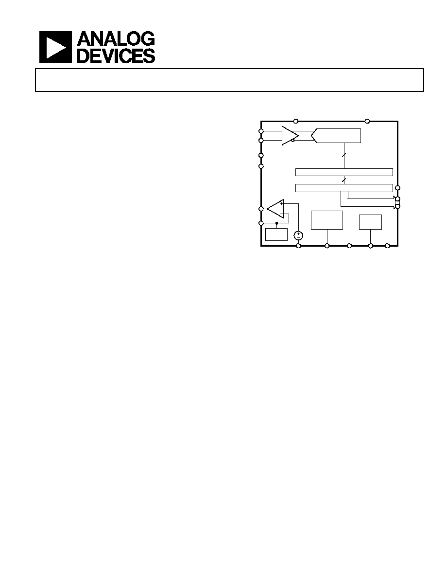
FUNCTIONAL BLOCK DIAGRAM
SHA
VIN+
VIN–
REFT
REFB
DRVDD
CLK
PDWN
MODE
CLOCK
DUTY CYCLE
STABLIZER
MODE
SELECT
DGND
OR
D9 (MSB)
02874-
A-
001
D0
AVDD
CORRECTION LOGIC
OUTPUT BUFFERS
10
REF
SELECT
AGND
0.5V
VREF
SENSE
AD9215
PIPELINE
ADC CORE
Figure 1.
PRODUCT DESCRIPTION
The AD9215 is a family of monolithic, single 3 V supply, 10-bit,
65/80/105 MSPS analog-to-digital converters (ADC). This family
features a high performance sample-and-hold amplifier (SHA)
and voltage reference. The AD9215 uses a multistage differential
pipelined architecture with output error correction logic to pro-
vide 10-bit accuracy at 105 MSPS data rates and to guarantee no
missing codes over the full operating temperature range.
The wide bandwidth, truly differential sample-and-hold ampli-
fier (SHA) allows for a variety of user-selectable input ranges
and offsets including single-ended applications. It is suitable for
multiplexed systems that switch full-scale voltage levels in
successive channels and for sampling single-channel inputs at
frequencies well beyond the Nyquist rate. Combined with pow-
er and cost savings over previously available ADCs, the AD9215
is suitable for applications in communications, imaging, and
medical ultrasound.
A single-ended clock input is used to control all internal conversion
cycles. A duty cycle stabilizer compensates for wide variations in the
clock duty cycle while maintaining excellent performance. The digital
output data is presented in straight binary or twos complement for-
mats. An out-of-range signal indicates an overflow condition, which
can be used with the MSB to determine low or high overflow.
Fabricated on an advanced CMOS process, the AD9215 is avail-
able in both a 28-lead surface-mount plastic package and a
32-lead chip scale package and is specified over the industrial
temperature range of 40°C to +85°C.
PRODUCT HIGHLIGHTS
1.
The AD9215 operates from a single 3 V power supply and
features a separate digital output driver supply to accom-
modate 2.5 V and 3.3 V logic families.
2.
Operating at 105 MSPS, the AD9215 core ADC consumes
a low 120 mW; at 80 MSPS, the power dissipation is 104
mW; and at 65 MSPS, the power dissipation is 96 mW.
3.
The patented SHA input maintains excellent performance
for input frequencies up to 200 MHz and can be config-
ured for single-ended or differential operation.
4.
The AD9215 is part of several pin compatible 10-, 12-, and
14-bit low power ADCs. This allows a simplified upgrade
from 10 bits to 12 bits for systems up to 80 MSPS.
5.
The clock duty cycle stabilizer maintains converter per-
formance over a wide range of clock pulse widths.
6.
The out of range (OR) output bit indicates when the signal
is beyond the selected input range.
相关PDF资料 |
PDF描述 |
|---|---|
| MAX3317CUP+ | TXRX RS232 2.5V 460KBPS 20TSSOP |
| MS27467E15F35PA | CONN PLUG 37POS STRAIGHT W/PINS |
| V150B12M150B2 | CONVERTER MOD DC/DC 12V 150W |
| AD9214BRS-105 | IC ADC 10BIT 105MSPS 3V 28-SSOP |
| MS27472E12F35P | CONN RCPT 22POS WALL MNT W/PINS |
相关代理商/技术参数 |
参数描述 |
|---|---|
| AD9215BRU-65EB | 制造商:Analog Devices 功能描述:Evaluation Board For AD9215 3 V A/D Converter ,10-Bit, 65/80/105 MSPS 制造商:Analog Devices 功能描述:EVAL BD FOR AD9215 3V A/D CNVRTR ,10-BIT, 65/80/105 MSPS - Rail/Tube |
| AD9215BRU-80 | 功能描述:IC ADC 10BIT 80MSPS 3V 28-TSSOP RoHS:否 类别:集成电路 (IC) >> 数据采集 - 模数转换器 系列:- 产品培训模块:Lead (SnPb) Finish for COTS Obsolescence Mitigation Program 标准包装:2,500 系列:- 位数:12 采样率(每秒):3M 数据接口:- 转换器数目:- 功率耗散(最大):- 电压电源:- 工作温度:- 安装类型:表面贴装 封装/外壳:SOT-23-6 供应商设备封装:SOT-23-6 包装:带卷 (TR) 输入数目和类型:- |
| AD9215BRU-80EB | 制造商:Analog Devices 功能描述:Evaluation Board For AD9215 3 V A/D Converter ,10-Bit, 65/80/105 MSPS 制造商:Analog Devices 功能描述:EVAL BD FOR AD9215 3V A/D CNVRTR ,10-BIT, 65/80/105 MSPS - Rail/Tube |
| AD9215BRURL7-105 | 制造商:AD 制造商全称:Analog Devices 功能描述:10-Bit, 65/80/105 MSPS, 3V A/D Converter |
| AD9215BRURL7-65 | 制造商:Rochester Electronics LLC 功能描述: 制造商:Analog Devices 功能描述: |
发布紧急采购,3分钟左右您将得到回复。