- 您现在的位置:买卖IC网 > PDF目录10532 > AD9218BSTZ-80 (Analog Devices Inc)IC ADC 10BIT DUAL 80MSPS 48-LQFP PDF资料下载
参数资料
| 型号: | AD9218BSTZ-80 |
| 厂商: | Analog Devices Inc |
| 文件页数: | 10/28页 |
| 文件大小: | 0K |
| 描述: | IC ADC 10BIT DUAL 80MSPS 48-LQFP |
| 标准包装: | 1 |
| 位数: | 10 |
| 采样率(每秒): | 80M |
| 数据接口: | 并联 |
| 转换器数目: | 2 |
| 功率耗散(最大): | 525mW |
| 电压电源: | 模拟和数字 |
| 工作温度: | -40°C ~ 85°C |
| 安装类型: | 表面贴装 |
| 封装/外壳: | 48-LQFP |
| 供应商设备封装: | 48-LQFP(7x7) |
| 包装: | 托盘 |
| 输入数目和类型: | 2 个差分,单极 |
第1页第2页第3页第4页第5页第6页第7页第8页第9页当前第10页第11页第12页第13页第14页第15页第16页第17页第18页第19页第20页第21页第22页第23页第24页第25页第26页第27页第28页
AD9218
Rev. C | Page 18 of 28
THEORY OF OPERATION
ANALOG INPUT
The AD9218 ADC architecture is a bit-per-stage pipeline-type
converter utilizing switch capacitor techniques. These stages
determine the 7 MSBs and drive a 3-bit flash. Each stage
provides sufficient overlap and error correction, allowing
optimization of comparator accuracy. The input buffers are
differential, and both sets of inputs are internally biased. This
allows the most flexible use of ac-coupled or dc-coupled and
differential or single-ended input modes. The output staging
block aligns the data, carries out the error correction, and feeds
the data to output buffers. The set of output buffers are powered
from a separate supply, allowing adjustment of the output
voltage swing. There is no discernible difference in performance
between the two channels.
The analog input to the AD9218 is a differential buffer. For best
dynamic performance, impedance at A
AIN
and
IN
should match.
Special care was taken in the design of the analog input section
of the AD9218 to prevent damage and data corruption when
the input is overdriven. The nominal input range is 1.024 V p-p.
Optimum performance is obtained when the part is driven
differentially where common-mode noise is minimized and
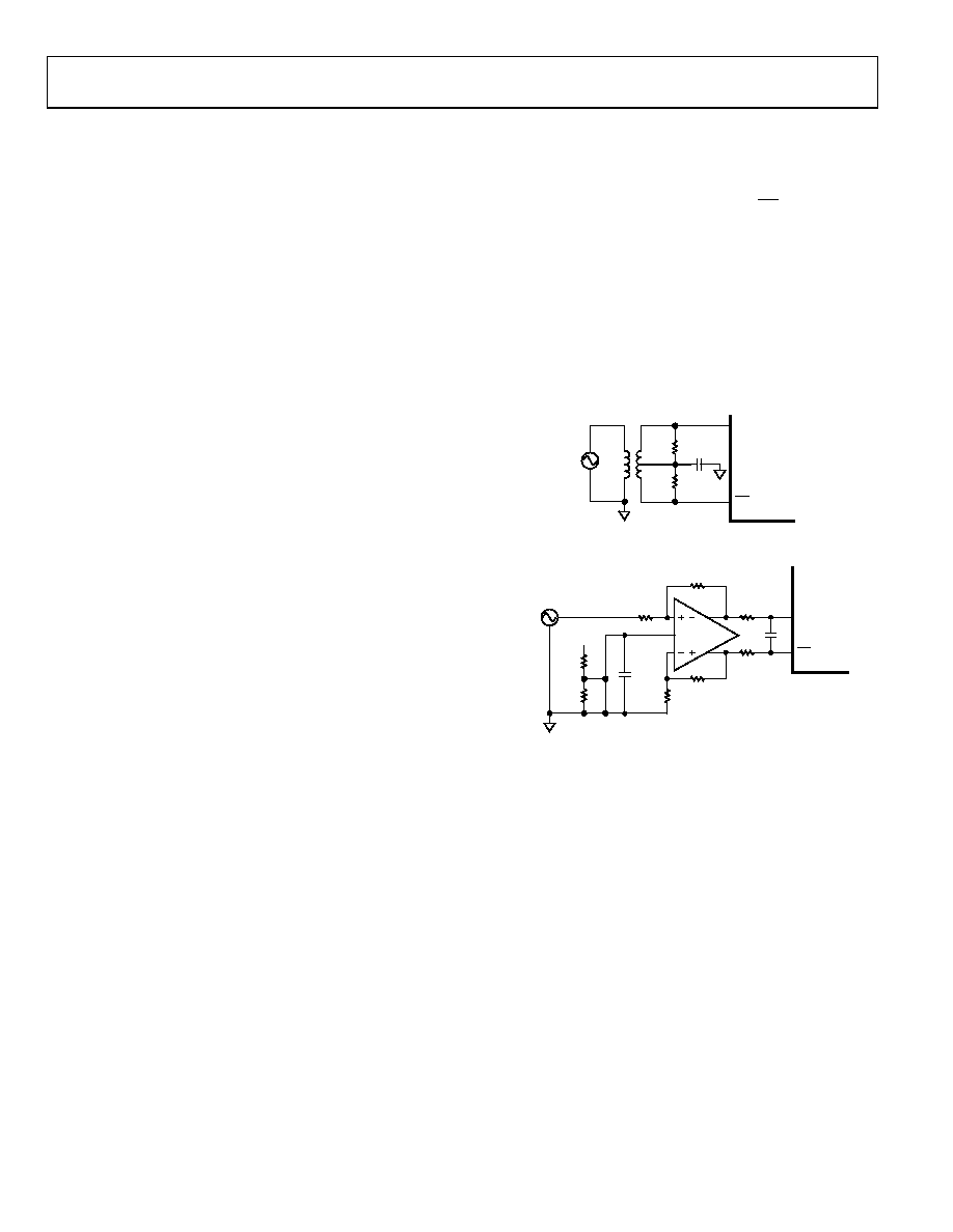
even-order harmonics are reduced. Figure 42 shows an example
of the AD9218 being driven differentially via a wideband RF
transformer for ac-coupled applications. As shown in Figure 43,
applications that require dc-coupled differential drives can be
accommodated using the AD8138 differential output op amp.
USING THE AD9218 ENCODE INPUT
02
00
1-
04
2
AD9218
50
ANALOG
SIGNAL
SOURCE
AIN
25
0.1F
1:1
Any high speed ADC is extremely sensitive to the quality of the
sampling clock provided by the user. A track-and-hold circuit is
essentially a mixer. Any noise, distortion, or timing jitter on the
clock is combined with the desired signal at the analog-to-
digital output. For that reason, considerable care has been taken
in the design of the ENCODE input of the AD9218, and the
user is advised to give commensurate thought to the clock
source. The ENCODE input is fully TTL/CMOS compatible.
Figure 42. Using a Wideband Transformer to Drive the AD9218
02
00
1-
04
3
AD9218
50
ANALOG
SIGNAL
SOURCE
AIN
10k
5k
AVDD
0.1F
500
525
AD8138
VOCM
15pF
25
DIGITAL OUTPUTS
The digital outputs are TTL/CMOS compatible for lower power
consumption. During power-down, the output buffers transition to
a high impedance state. A data format selection option supports
either twos complement (set high) or offset binary output (set
low) formats.
Figure 43. Using the AD8138 to Drive the AD9218
相关PDF资料 |
PDF描述 |
|---|---|
| VI-B53-MX-F3 | CONVERTER MOD DC/DC 24V 75W |
| LTC2292CUP#PBF | IC ADC DUAL 12BIT 40MSPS 64QFN |
| VE-J5F-MY-F4 | CONVERTER MOD DC/DC 72V 50W |
| VE-J3W-MY-F2 | CONVERTER MOD DC/DC 5.5V 50W |
| AD7675ASTZ | IC ADC 16BIT DIFF INP 48LQFP |
相关代理商/技术参数 |
参数描述 |
|---|---|
| AD9218BSTZ-801 | 制造商:AD 制造商全称:Analog Devices 功能描述:10-Bit, 40/65/80/105 MSPS 3 V Dual Analog-to-Digital Converter |
| AD9218BSTZ-RL105 | 功能描述:IC ADC 10BIT DUAL 105MSPS 48LQFP RoHS:是 类别:集成电路 (IC) >> 数据采集 - 模数转换器 系列:- 标准包装:1 系列:- 位数:14 采样率(每秒):83k 数据接口:串行,并联 转换器数目:1 功率耗散(最大):95mW 电压电源:双 ± 工作温度:0°C ~ 70°C 安装类型:通孔 封装/外壳:28-DIP(0.600",15.24mm) 供应商设备封装:28-PDIP 包装:管件 输入数目和类型:1 个单端,双极 |
| AD9218BSTZ-RL1051 | 制造商:AD 制造商全称:Analog Devices 功能描述:10-Bit, 40/65/80/105 MSPS 3 V Dual Analog-to-Digital Converter |
| AD9218BSTZ-RL40 | 功能描述:IC ADC 10BIT DUAL 40MSPS 48-LQFP RoHS:是 类别:集成电路 (IC) >> 数据采集 - 模数转换器 系列:- 标准包装:1,000 系列:- 位数:12 采样率(每秒):300k 数据接口:并联 转换器数目:1 功率耗散(最大):75mW 电压电源:单电源 工作温度:0°C ~ 70°C 安装类型:表面贴装 封装/外壳:24-SOIC(0.295",7.50mm 宽) 供应商设备封装:24-SOIC 包装:带卷 (TR) 输入数目和类型:1 个单端,单极;1 个单端,双极 |
| AD9218BSTZ-RL401 | 制造商:AD 制造商全称:Analog Devices 功能描述:10-Bit, 40/65/80/105 MSPS 3 V Dual Analog-to-Digital Converter |
发布紧急采购,3分钟左右您将得到回复。