- 您现在的位置:买卖IC网 > PDF目录373960 > AD9221 (Analog Devices, Inc.) Complete 12-Bit 1.5/3.0/10.0 MSPS Monolithic A/D Converters PDF资料下载
参数资料
| 型号: | AD9221 |
| 厂商: | Analog Devices, Inc. |
| 元件分类: | 串行ADC |
| 英文描述: | Complete 12-Bit 1.5/3.0/10.0 MSPS Monolithic A/D Converters |
| 中文描述: | 完整的12位1.5/3.0/10.0 MSPS的单片的A / D转换器 |
| 文件页数: | 18/28页 |
| 文件大小: | 350K |
| 代理商: | AD9221 |
第1页第2页第3页第4页第5页第6页第7页第8页第9页第10页第11页第12页第13页第14页第15页第16页第17页当前第18页第19页第20页第21页第22页第23页第24页第25页第26页第27页第28页
AD9221/AD9223/AD9220
REV. D
–18–
SFDR over a wide range of amplitudes required by the most
demanding communication applications. Similar performance is
achievable with the AD9221 and AD9223 at their correspond-
ing Nyquist frequency.
INPUT AMPLITUDE – dBFS
90
20
–50
0
S
–40
–30
–20
–10
80
70
30
60
50
40
SNR – 2.0V p-p
SNR – 5.0V p-p
SFDR – 5.0V p-p
SFDR – 2.0V p-p
Figure 46. AD9220 SFDR, SNR vs. Input Amplitude
(f
IN
= 5 MHz, f
CLK
= 10 MSPS, V
CM
= 2.5 V, Differential)
Figure 46 also reveals a noteworthy difference in the SFDR and
SNR performance of the AD9220 between the 2 V p-p and 5 V
p-p input span options. First, the SNR performance improves
by 2 dB with a 5.0 V p-p input span due to the increase in dy-
namic range. Second, the SFDR performance of the AD9220
will improve for input signals below approximately –6.0 dBFS.
A 3 dB to 5 dB improvement was typically realized for input
signal levels between –6.0 dBFS and –36 dBFS. This improve-
ment in SNR and SFDR for a 5.0 V p-p span may be advanta-
geous for communication systems that have additional margin
or headroom to minimize clipping of the ADC.
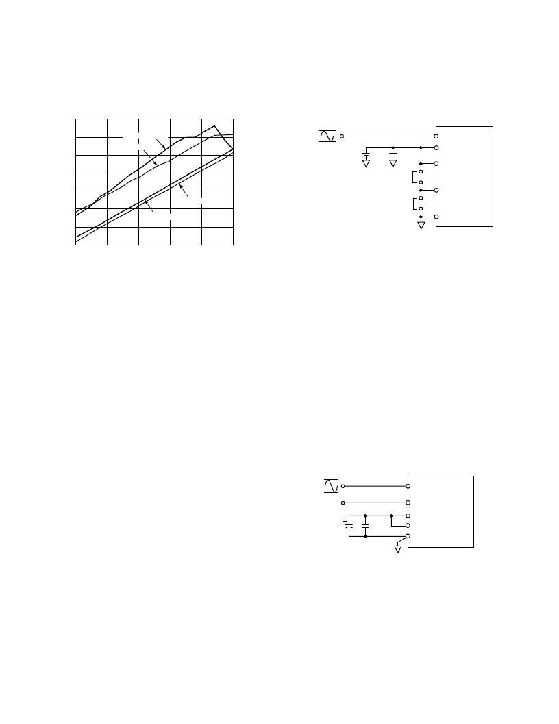
REFERENCE CONFIGURATIONS
The figures associated with this section on internal and external
reference operation do not show recommended matching series resistors
for VINA and VINB for the purpose of simplicity. Please refer to
section Driving the Analog Inputs, Introduction for a discussion of
this topic. Also, the figures do not show the decoupling network asso-
ciated with the CAPT and CAPB pins. Please refer to the section “Ref-
erence Operation” for a discussion of the internal reference circuitry
and the recommended decoupling network shown in Figure 36.
USING THE INTERNAL REFERENCE
Single-Ended Input with 0 to 2
3
VREF Range
Figure 47 shows how to connect the AD9221/AD9223/AD9220
for a 0 V to 2 V or 0 V to 5 V input range via pin strapping the
SENSE pin. An intermediate input range of 0 to 2
×
VREF can
be established using the resistor programmable configuration in
Figure 49 and connecting VREF to VINB.
In either case, both the common-mode voltage and input span
are directly dependent on the value of VREF. More specifically,
the common-mode voltage is equal to VREF while the input
span is equal to 2
×
VREF. Thus, the valid input range extends
from 0 to 2
×
VREF. When VINA is
≤
0 V, the digital output
will be 000 Hex; when VINA is
≥
2
×
VREF, the digital output
will be FFF Hex.
Shorting the VREF pin directly to the SENSE pin places the
internal reference amplifier in unity-gain mode and the resultant
VREF output is 1 V. Therefore, the valid input range is 0 V to
2V. However, shorting the SENSE pin directly to the REFCOM
pin configures the internal reference amplifier for a gain of 2.5
and the resultant VREF output is 2.5 V. Thus, the valid input
range becomes 0 V to 5 V. The VREF pin should be bypassed
to the REFCOM pin with a 10
μ
F tantalum capacitor in parallel
with a low-inductance 0.1
μ
F ceramic capacitor.
10
m
F
VINA
VREF
0.1
m
F
VINB
2
3
VREF
0V
SHORT FOR 0V TO 2V
INPUT SPAN
SENSE
SHORT FOR 0V TO 5V
INPUT SPAN
REFCOM
AD9221/
AD9223/
AD9220
Figure 47. Internal Reference—2 V p-p Input Span, V
CM
=
1 V, or 5 V p-p Input Span, V
CM
= 2.5 V
Single-Ended or Differential Input, V
CM
= 2.5 V
Figure 48 shows the single-ended configuration that gives the
best dynamic performance (SINAD, SFDR). To optimize
dynamic specifications, center the common-mode voltage of the
analog input at approximately by 2.5 V by connecting VINB to
a low-impedance 2.5 V source. As described above, shorting
the VREF pin directly to the SENSE pin results in a 1 V refer-
ence voltage and a 2 V p-p input span. The valid range for
input signals is 1.5 V to 3.5 V. The VREF pin should be by-
passed to the REFCOM pin with a 10
μ
F tantalum capacitor in
parallel with a low-inductance 0.1
μ
F ceramic capacitor.
This reference configuration could also be used for a differential
input in which VINA and VINB are driven via a transformer as
shown in Figure 45. In this case, the common-mode voltage,
V
CM
, is set at midsupply by connecting the transformers center
tap to CML of the AD9221/AD9223/AD9220. VREF can be
configured for 1 V or 2.5 V by connecting SENSE to either
VREF or REFCOM respectively. Note that the valid input
range for each of the differential input is one half of the single-
ended input and thus becomes V
CM
– VREF/2 to V
CM
+ VREF/2.
1V
0.1
m
F
10
m
F
VINA
VINB
VREF
SENSE
REFCOM
3.5V
1.5V
2.5V
AD9221/
AD9223/
AD9220
Figure 48. Internal Reference—2 V p-p Input Span,
V
CM
= 2.5 V
Resistor Programmable Reference
Figure 49 shows an example of how to generate a reference
voltage other than 1 V or 2.5 V with the addition of two exter-
nal resistors and a bypass capacitor. Use the equation,
VREF
= 1
V
×
(1 +
R
1/
R
2),
to determine appropriate values for
R
1 and
R
2. These resistors
should be in the 2 k
to 100 k
range. For the example shown,
R1 equals 2.5 k
and R2 equals 5 k
. From the equation
above, the resultant reference voltage on the VREF pin is
相关PDF资料 |
PDF描述 |
|---|---|
| AD9221AR | RES, 18.2K, 1/4, 1%, MF |
| AD9221ARS | Complete 12-Bit 1.5/3.0/10.0 MSPS Monolithic A/D Converters |
| AD9223 | Complete 12-Bit 1.5/3.0/10.0 MSPS Monolithic A/D Converters |
| AD9223AR | Complete 12-Bit 1.5/3.0/10.0 MSPS Monolithic A/D Converters |
| AD9224ARS | Complete 12-Bit 40 MSPS Monolithic A/D Converter |
相关代理商/技术参数 |
参数描述 |
|---|---|
| AD9221AR | 功能描述:IC ADC 12BIT 1.5MSPS 28-SOIC RoHS:否 类别:集成电路 (IC) >> 数据采集 - 模数转换器 系列:- 标准包装:1,000 系列:- 位数:12 采样率(每秒):300k 数据接口:并联 转换器数目:1 功率耗散(最大):75mW 电压电源:单电源 工作温度:0°C ~ 70°C 安装类型:表面贴装 封装/外壳:24-SOIC(0.295",7.50mm 宽) 供应商设备封装:24-SOIC 包装:带卷 (TR) 输入数目和类型:1 个单端,单极;1 个单端,双极 |
| AD9221AR-REEL | 功能描述:IC ADC 12BIT 1.5MSPS 28-SOIC RoHS:否 类别:集成电路 (IC) >> 数据采集 - 模数转换器 系列:- 标准包装:1,000 系列:- 位数:12 采样率(每秒):300k 数据接口:并联 转换器数目:1 功率耗散(最大):75mW 电压电源:单电源 工作温度:0°C ~ 70°C 安装类型:表面贴装 封装/外壳:24-SOIC(0.295",7.50mm 宽) 供应商设备封装:24-SOIC 包装:带卷 (TR) 输入数目和类型:1 个单端,单极;1 个单端,双极 |
| AD9221ARS | 功能描述:IC ADC 12BIT 1.5MSPS 28-SSOP RoHS:否 类别:集成电路 (IC) >> 数据采集 - 模数转换器 系列:- 标准包装:1,000 系列:- 位数:12 采样率(每秒):300k 数据接口:并联 转换器数目:1 功率耗散(最大):75mW 电压电源:单电源 工作温度:0°C ~ 70°C 安装类型:表面贴装 封装/外壳:24-SOIC(0.295",7.50mm 宽) 供应商设备封装:24-SOIC 包装:带卷 (TR) 输入数目和类型:1 个单端,单极;1 个单端,双极 |
| AD9221ARS-REEL | 功能描述:IC ADC 12BIT 1.5MSPS 28-SSOP RoHS:否 类别:集成电路 (IC) >> 数据采集 - 模数转换器 系列:- 标准包装:1,000 系列:- 位数:12 采样率(每秒):300k 数据接口:并联 转换器数目:1 功率耗散(最大):75mW 电压电源:单电源 工作温度:0°C ~ 70°C 安装类型:表面贴装 封装/外壳:24-SOIC(0.295",7.50mm 宽) 供应商设备封装:24-SOIC 包装:带卷 (TR) 输入数目和类型:1 个单端,单极;1 个单端,双极 |
| AD9221ARSZ | 功能描述:IC ADC 12BIT 1.5MSPS 28SSOP RoHS:是 类别:集成电路 (IC) >> 数据采集 - 模数转换器 系列:- 标准包装:1,000 系列:- 位数:12 采样率(每秒):300k 数据接口:并联 转换器数目:1 功率耗散(最大):75mW 电压电源:单电源 工作温度:0°C ~ 70°C 安装类型:表面贴装 封装/外壳:24-SOIC(0.295",7.50mm 宽) 供应商设备封装:24-SOIC 包装:带卷 (TR) 输入数目和类型:1 个单端,单极;1 个单端,双极 |
发布紧急采购,3分钟左右您将得到回复。