- 您现在的位置:买卖IC网 > PDF目录373960 > AD9223ARS (ANALOG DEVICES INC) Complete 12-Bit 1.5/3.0/10.0 MSPS Monolithic A/D Converters PDF资料下载
参数资料
| 型号: | AD9223ARS |
| 厂商: | ANALOG DEVICES INC |
| 元件分类: | ADC |
| 英文描述: | Complete 12-Bit 1.5/3.0/10.0 MSPS Monolithic A/D Converters |
| 中文描述: | 1-CH 12-BIT FLASH METHOD ADC, PARALLEL ACCESS, PDSO28 |
| 封装: | MO-150AH, SSOP-28 |
| 文件页数: | 5/28页 |
| 文件大小: | 350K |
| 代理商: | AD9223ARS |
第1页第2页第3页第4页当前第5页第6页第7页第8页第9页第10页第11页第12页第13页第14页第15页第16页第17页第18页第19页第20页第21页第22页第23页第24页第25页第26页第27页第28页
AD9221/AD9223/AD9220
REV. D
–5–
ZERO ERROR
The major carry transition should occur for an analog value
1/2 LSB below VINA = VINB. Zero error is defined as the
deviation of the actual transition from that point.
GAIN ERROR
The first code transition should occur at an analog value
1/2 LSB above negative full scale. The last transition should
occur at an analog value 1 1/2 LSB below the nominal full
scale. Gain error is the deviation of the actual difference
between first and last code transitions and the ideal differ-
ence between first and last code transitions.
TEMPERATURE DRIFT
The temperature drift for zero error and gain error specifies the
maximum change from the initial (+25
°
C) value to the value at
T
MIN
or T
MAX
.
POWER SUPPLY REJECTION
The specification shows the maximum change in full scale from
the value with the supply at the minimum limit to the value
with the supply at its maximum limit.
APERTURE JITTER
Aperture jitter is the variation in aperture delay for successive
samples and is manifested as noise on the input to the A/D.
APERTURE DELAY
Aperture delay is a measure of the sample-and-hold amplifier
(SHA) performance and is measured from the rising edge of the
clock input to when the input signal is held for conversion.
SIGNAL-TO-NOISE AND DISTORTION (S/N+D, SINAD)
RATIO
S/N+D is the ratio of the rms value of the measured input sig-
nal to the rms sum of all other spectral components below the
Nyquist frequency, including harmonics but excluding dc.
The value for S/N+D is expressed in decibels.
EFFECTIVE NUMBER OF BITS (ENOB)
For a sine wave, SINAD can be expressed in terms of the num-
ber of bits. Using the following formula,
N
= (
SINAD
– 1.76)/6.02
it is possible to get a measure of performance expressed as
N
,
the effective number of bits.
Thus, effective number of bits for a device for sine wave inputs
at a given input frequency can be calculated directly from its
measured SINAD.
TOTAL HARMONIC DISTORTION (THD)
THD is the ratio of the rms sum of the first six harmonic
components to the rms value of the measured input signal and
is expressed as a percentage or in decibels.
SIGNAL-TO-NOISE RATIO (SNR)
SNR is the ratio of the rms value of the measured input signal
to the rms sum of all other spectral components below the
Nyquist frequency, excluding the first six harmonics and dc.
The value for SNR is expressed in decibels.
SPURIOUS FREE DYNAMIC RANGE (SFDR)
SFDR is the difference in dB between the rms amplitude of the
input signal and the peak spurious signal.
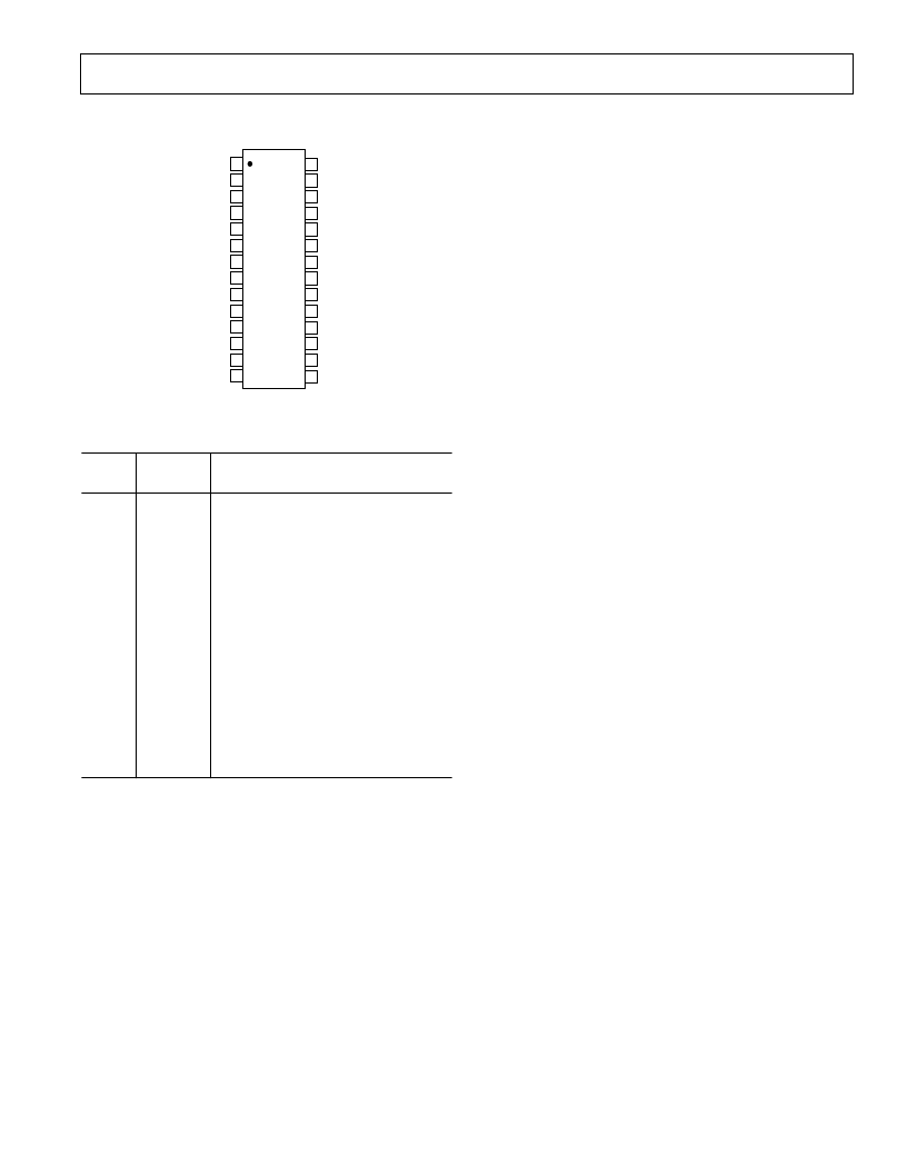
PIN CONNECTIONS
14
13
12
11
17
16
15
20
19
18
10
9
8
1
2
3
4
7
6
5
TOP VIEW
(Not to Scale)
28
27
26
25
24
23
22
21
AD9221/
AD9223/
AD9220
CLK
AVSS
AVDD
DVSS
DVDD
(LSB) BIT 12
BIT 11
BIT 10
CML
VINA
VINB
BIT 9
BIT 8
BIT 7
BIT 6
BIT 5
BIT 4
REFCOM
CAPB
CAPT
BIT 3
BIT 2
(MSB) BIT 1
OTR
VREF
AVDD
AVSS
SENSE
PIN FUNCTION DESCRIPTIONS
Pin
Number Name
Description
1
2
3–12
13
14
15, 26
16, 25
17
18
19
20
21
22
23
24
27
28
CLK
BIT 12
BIT N
BIT 1
OTR
AVDD
AVSS
SENSE
VREF
REFCOM
CAPB
CAPT
CML
VINA
VINB
DVSS
DVDD
Clock Input Pin
Least Significant Data Bit (LSB)
Data Output Bit
Most Significant Data Bit (MSB)
Out of Range
+5 V Analog Supply
Analog Ground
Reference Select
Reference I/O
Reference Common
Noise Reduction Pin
Noise Reduction Pin
Common-Mode Level (Midsupply)
Analog Input Pin (+)
Analog Input Pin (–)
Digital Ground
+3 V to +5 V Digital Supply
DEFINITIONS OF SPECIFICATION
INTEGRAL NONLINEARITY (INL)
INL refers to the deviation of each individual code from a line
drawn from “negative full scale” through “positive full scale.”
The point used as “negative full scale” occurs 1/2 LSB before
the first code transition. “Positive full scale” is defined as a
level 1 1/2 LSB beyond the last code transition. The deviation
is measured from the middle of each particular code to the true
straight line.
DIFFERENTIAL NONLINEARITY (DNL, NO MISSING
CODES)
An ideal ADC exhibits code transitions that are exactly 1 LSB
apart. DNL is the deviation from this ideal value. Guaranteed
no missing codes to 12-bit resolution indicates that all 4096
codes, respectively, must be present over all operating ranges.
相关PDF资料 |
PDF描述 |
|---|---|
| AD9220AR | Complete 12-Bit 1.5/3.0/10.0 MSPS Monolithic A/D Converters |
| AD9220ARS | Complete 12-Bit 1.5/3.0/10.0 MSPS Monolithic A/D Converters |
| AD9221 | Complete 12-Bit 1.5/3.0/10.0 MSPS Monolithic A/D Converters |
| AD9221AR | RES, 18.2K, 1/4, 1%, MF |
| AD9221ARS | Complete 12-Bit 1.5/3.0/10.0 MSPS Monolithic A/D Converters |
相关代理商/技术参数 |
参数描述 |
|---|---|
| AD9223ARS-REEL | 制造商:Analog Devices 功能描述:ADC Single Pipelined 3Msps 12-bit Parallel 28-Pin SSOP T/R |
| AD9223ARSZ | 功能描述:IC ADC 12BIT 3.0MSPS 28-SSOP RoHS:是 类别:集成电路 (IC) >> 数据采集 - 模数转换器 系列:- 标准包装:1 系列:microPOWER™ 位数:8 采样率(每秒):1M 数据接口:串行,SPI? 转换器数目:1 功率耗散(最大):- 电压电源:模拟和数字 工作温度:-40°C ~ 125°C 安装类型:表面贴装 封装/外壳:24-VFQFN 裸露焊盘 供应商设备封装:24-VQFN 裸露焊盘(4x4) 包装:Digi-Reel® 输入数目和类型:8 个单端,单极 产品目录页面:892 (CN2011-ZH PDF) 其它名称:296-25851-6 |
| AD9223ARSZ-REEL | 功能描述:IC ADC 12BIT 3.0MSPS 28SSOP RoHS:是 类别:集成电路 (IC) >> 数据采集 - 模数转换器 系列:- 标准包装:1,000 系列:- 位数:12 采样率(每秒):300k 数据接口:并联 转换器数目:1 功率耗散(最大):75mW 电压电源:单电源 工作温度:0°C ~ 70°C 安装类型:表面贴装 封装/外壳:24-SOIC(0.295",7.50mm 宽) 供应商设备封装:24-SOIC 包装:带卷 (TR) 输入数目和类型:1 个单端,单极;1 个单端,双极 |
| AD9223ARZ | 功能描述:IC ADC 12BIT 3.0MSPS 28SOIC RoHS:是 类别:集成电路 (IC) >> 数据采集 - 模数转换器 系列:- 其它有关文件:TSA1204 View All Specifications 标准包装:1 系列:- 位数:12 采样率(每秒):20M 数据接口:并联 转换器数目:2 功率耗散(最大):155mW 电压电源:模拟和数字 工作温度:-40°C ~ 85°C 安装类型:表面贴装 封装/外壳:48-TQFP 供应商设备封装:48-TQFP(7x7) 包装:Digi-Reel® 输入数目和类型:4 个单端,单极;2 个差分,单极 产品目录页面:1156 (CN2011-ZH PDF) 其它名称:497-5435-6 |
| AD9223ARZ-REEL | 功能描述:IC ADC 12BIT 3.0MSPS 28SOIC RoHS:是 类别:集成电路 (IC) >> 数据采集 - 模数转换器 系列:- 标准包装:1,000 系列:- 位数:12 采样率(每秒):300k 数据接口:并联 转换器数目:1 功率耗散(最大):75mW 电压电源:单电源 工作温度:0°C ~ 70°C 安装类型:表面贴装 封装/外壳:24-SOIC(0.295",7.50mm 宽) 供应商设备封装:24-SOIC 包装:带卷 (TR) 输入数目和类型:1 个单端,单极;1 个单端,双极 |
发布紧急采购,3分钟左右您将得到回复。