- 您现在的位置:买卖IC网 > PDF目录10534 > AD9223ARZ (Analog Devices Inc)IC ADC 12BIT 3.0MSPS 28SOIC PDF资料下载
参数资料
| 型号: | AD9223ARZ |
| 厂商: | Analog Devices Inc |
| 文件页数: | 3/32页 |
| 文件大小: | 0K |
| 描述: | IC ADC 12BIT 3.0MSPS 28SOIC |
| 标准包装: | 27 |
| 位数: | 12 |
| 采样率(每秒): | 3M |
| 数据接口: | 并联 |
| 转换器数目: | 7 |
| 功率耗散(最大): | 130mW |
| 电压电源: | 单电源 |
| 工作温度: | -40°C ~ 85°C |
| 安装类型: | 表面贴装 |
| 封装/外壳: | 28-SOIC(0.295",7.50mm 宽) |
| 供应商设备封装: | 28-SOIC W |
| 包装: | 管件 |
| 输入数目和类型: | 2 个单端,单极;1 个差分,单极 |
第1页第2页当前第3页第4页第5页第6页第7页第8页第9页第10页第11页第12页第13页第14页第15页第16页第17页第18页第19页第20页第21页第22页第23页第24页第25页第26页第27页第28页第29页第30页第31页第32页
REV. E
AD9221/AD9223/AD9220
–11–
Referring to Figure 5, the differential SHA is implemented using a
switched-capacitor topology. Therefore, its input impedance
and its subsequent effects on the input drive source should be
understood to maximize the converter’s performance. The com-
bination of the pin capacitance, CPIN, parasitic capacitance, CPAR,
and sampling capacitance, CS, is typically less than 16 pF.
When the SHA goes into track mode, the input source must
charge or discharge the voltage stored on CS to the new input
voltage. This action of charging and discharging CS, averaged
over a period of time and for a given sampling frequency, fS,
makes the input impedance appear to have a benign resistive
component. However, if this action is analyzed within a sampling
period (i.e., T = 1/fS), the input impedance is dynamic and there-
fore certain precautions on the input drive source should be
observed.
The resistive component to the input impedance can be com-
puted by calculating the average charge that gets drawn by CH
from the input drive source. It can be shown that if CS is allowed
to fully charge up to the input voltage before switches QS1 are
opened, then the average current into the input is the same as if
there were a resistor of 1/(CS fS) ohms connected between the
inputs. This means that the input impedance is inversely pro-
portional to the converter’s sample rate. Since CS is only 4 pF,
this resistive component is typically much larger than that of the
drive source (i.e., 25 k
at f
S = 10 MSPS).
If one considers the SHA’s input impedance over a sampling
period, it appears as a dynamic input impedance to the input
drive source. When the SHA goes into the track mode, the input
source should ideally provide the charging current through RON
of switch QS1 in an exponential manner. The requirement of
exponential charging means that the most common input source,
an op amp, must exhibit a source impedance that is both low
and resistive up to and beyond the sampling frequency.
The output impedance of an op amp can be modeled with a
series inductor and resistor. When a capacitive load is switched
onto the output of the op amp, the output will momentarily
drop due to its effective output impedance. As the output recov-
ers, ringing may occur. To remedy the situation, a series resistor
can be inserted between the op amp and the SHA input as shown
in Figure 7. The series resistance helps isolate the op amp from
the switched-capacitor load.
10 F
VINA
VINB
SENSE
AD9221/AD9223/
AD9220
0.1 F
RS
VCC
VEE
RS
VREF
REFCOM
Figure 7. Series Resistor Isolates Switched-Capacitor SHA
Input from Op Amp. Matching Resistors Improve SNR
Performance
The optimum size of this resistor is dependent on several factors,
which include the AD9221/AD9223/AD9220 sampling rate, the
selected op amp, and the particular application. In most applica-
tions, a 30
to 50 resistor is sufficient. However, some
applications may require a larger resistor value to reduce the noise
bandwidth or possibly limit the fault current in an overvoltage
condition. Other applications may require a larger resistor value
as part of an antialiasing filter. In any case, since the THD
performance is dependent on the series resistance and the above
mentioned factors, optimizing this resistor value for a given
application is encouraged.
A slight improvement in SNR performance and dc offset
performance is achieved by matching the input resistance of VINA
and VINB. The degree of improvement is dependent on the
resistor value and the sampling rate. For series resistor values
greater than 100
, the use of a matching resistor is encouraged.
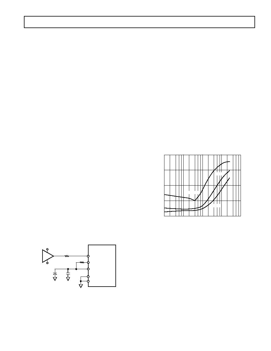
Figure 8 shows a plot for THD performance versus RSERIES for
the AD9221/AD9223/AD9220 at their respective sampling rate
and Nyquist frequency. The Nyquist frequency typically repre-
sents the worst case scenario for an ADC. In this case, a high
speed, high performance amplifier (AD8047) was used as the
buffer op amp. Although not shown, the AD9221/AD9223/AD9220
exhibits a slight increase in SNR (i.e. 1 dB to 1.5 dB) as the
resistance is increased from 0 k
to 2.56 k due to its bandlimiting
effect on wideband noise. Conversely, it exhibits slight decrease
in SNR (i.e., 0.5 dB to 2 dB) if VINA and VINB do not have a
matched input resistance.
RSERIES –
–45
–55
–85
1
10k
10
THD
–
dB
100
1k
–65
–75
AD9220
AD9223
AD9221
Figure 8. THD vs. RSERIES (fIN = fS / 2, AIN = –0.5 dB, Input
Span = 2 V p-p, VCM = 2.5 V)
Figure 8 shows that a small RSERIES between 30
and 50
provides the optimum THD performance for the AD9220.
Lower values of RSERIES are acceptable for the AD9223 and
AD9221 as their lower sampling rates provide a longer transient
recovery period for the AD8047. Note that op amps with lower
bandwidths will typically have a longer transient recovery period
and therefore require a slightly higher value of RSERIES and/or
lower sampling rate to achieve the optimum THD performance.
As the value of RSERIES increases, a corresponding increase in
distortion is noted. This is due to its interaction with the SHA’s
parasitic capacitor, CPAR, which has a signal dependency. Thus,
the resulting R-C time constant is signal dependent and conse-
quently a source of distortion.
The noise or small-signal bandwidth of the AD9221/AD9223/
AD9220 is the same as their full-power bandwidth as shown in
Figure 2. For noise sensitive applications, the excessive bandwidth
may be detrimental and the addition of a series resistor and/or
相关PDF资料 |
PDF描述 |
|---|---|
| HIN202EIBZ | IC 2DRVR/2RCVR RS232 5V 16-SOIC |
| VI-BT4-IV-F3 | CONVERTER MOD DC/DC 48V 150W |
| VI-BT4-IV-F1 | CONVERTER MOD DC/DC 48V 150W |
| AD9245BCPZ-20 | IC ADC 14BIT SGL 20MSPS 32LFCSP |
| TPA2016D2RTJT | IC AMP AUDIO PWR 2.8W D 20QFN |
相关代理商/技术参数 |
参数描述 |
|---|---|
| AD9223ARZ-REEL | 功能描述:IC ADC 12BIT 3.0MSPS 28SOIC RoHS:是 类别:集成电路 (IC) >> 数据采集 - 模数转换器 系列:- 标准包装:1,000 系列:- 位数:12 采样率(每秒):300k 数据接口:并联 转换器数目:1 功率耗散(最大):75mW 电压电源:单电源 工作温度:0°C ~ 70°C 安装类型:表面贴装 封装/外壳:24-SOIC(0.295",7.50mm 宽) 供应商设备封装:24-SOIC 包装:带卷 (TR) 输入数目和类型:1 个单端,单极;1 个单端,双极 |
| AD9223-EB | 制造商:Analog Devices 功能描述:EVAL KIT FOR COMPLETE 12-BIT 1.5/3.0/10.0MSPS MONOLITHIC A/D - Bulk |
| AD9224 | 制造商:AD 制造商全称:Analog Devices 功能描述:Complete 12-Bit 40 MSPS Monolithic A/D Converter |
| AD9224ARS | 制造商:Analog Devices 功能描述:Analog/Digital Converter IC Number of Bi |
| AD9224ARSZ | 功能描述:IC ADC 12BIT 40MSPS 28-SSOP RoHS:是 类别:集成电路 (IC) >> 数据采集 - 模数转换器 系列:- 标准包装:1 系列:microPOWER™ 位数:8 采样率(每秒):1M 数据接口:串行,SPI? 转换器数目:1 功率耗散(最大):- 电压电源:模拟和数字 工作温度:-40°C ~ 125°C 安装类型:表面贴装 封装/外壳:24-VFQFN 裸露焊盘 供应商设备封装:24-VQFN 裸露焊盘(4x4) 包装:Digi-Reel® 输入数目和类型:8 个单端,单极 产品目录页面:892 (CN2011-ZH PDF) 其它名称:296-25851-6 |
发布紧急采购,3分钟左右您将得到回复。