- 您现在的位置:买卖IC网 > PDF目录373960 > AD9224 (Analog Devices, Inc.) Complete 12-Bit 40 MSPS Monolithic A/D Converter PDF资料下载
参数资料
| 型号: | AD9224 |
| 厂商: | Analog Devices, Inc. |
| 英文描述: | Complete 12-Bit 40 MSPS Monolithic A/D Converter |
| 中文描述: | 完整的12位40 MSPS的单片A / D转换 |
| 文件页数: | 15/24页 |
| 文件大小: | 309K |
| 代理商: | AD9224 |
AD9224
–15–
REV. A
The driver circuit shown in Figure 23 is optimized for dc cou-
pling applications requiring optimum distortion performance.
This differential op amp driver circuit is configured to convert
and level shift a 2 V p-p single-ended, ground referenced signal
to a 4 V p-p differential signal centered at the VREF level of the
ADC. The circuit is based on two op amps that are configured
as matched unity gain difference amplifiers. The single-ended
input signal is applied to opposing inputs of the difference am-
plifiers, thus providing differential drive. The common-mode
offset voltage is applied to the noninverting resistor leg of each
difference amplifier providing the required offset voltage. The
common-mode offset can be varied over a wide span without
any serious degradation in distortion performance as shown in
Figure 25a, thus providing some flexibility in improving output
compression distortion from some
±
5 V op amps with limited
positive voltage swing.
To protect the AD9224 from an undervoltage fault condition
from op amps specified for
±
5 V operation, two diodes to AGND
can be inserted between each op amp output and the AD9224
inputs. The AD9224 will inherently be protected against any
overvoltage condition if the op amps share the same positive
power supply (i.e., AVDD) as the AD9224. Note, the gain
accuracy and common-mode rejection of each difference ampli-
fier in this driver circuit can be enhanced by using a matched thin-
film resistor network (i.e., Ohmtek ORNA5000F) for the op
amps. The AD9224’s small signal bandwidth is 120 MHz, hence
any noise falling within the baseband bandwidth of the AD9224
will degrade its overall noise performance.
The noise performance of each unity gain differential driver
circuit is limited by its inherent noise gain of two. For unity gain
op amps ONLY, the noise gain can be reduced from two to one
beyond the input signal’s passband by adding a shunt capacitor,
C
F
, across each op amp’s feedback resistor. This will essentially
establish a low-pass filter, which reduces the noise gain to one
beyond the filter’s f
–3 dB
while simultaneously bandlimiting the
input signal to f
–3 dB
. Note, the pole established by this filter
can also be used as the real pole of an antialiasing filter.
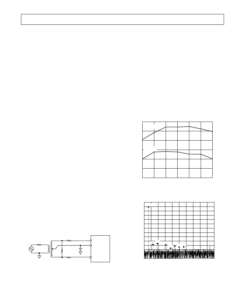
Figure 24 shows the schematic of the suggested transformer
circuit. The circuit uses a Minicircuits RF transformer, model
T4-1T, which has an impedance ratio of four (turns ratio of 2).
The schematic assumes that the signal source has a 50
source
impedance. The 1:4 impedance ratio requires the 200
sec-
ondary termination for optimum power transfer and VSWR.
The center tap of the transformer provides a convenient
means of level shifting the input signal to a desired common-
mode voltage.
VINA
VINB
AD9224
200
V
49.9
V
R
S
33
V
CML
MINICIRCUITS
T4-1T
0.1
m
F
R
S
33
V
Figure 24. Transformer Coupled Input
This (Figure 24) configuration was used to gather all of the
differential data on the Specifications pages.
Transformers with other turns ratios may also be selected to
optimize the performance of a given application. For example, a
given input signal source or amplifier may realize an improve-
ment in distortion performance at reduced output power levels
and signal swings. For example, selecting a transformer with a
higher impedance ratio (e.g., Minicircuits T16-6T with a 1:16
impedance ratio) effectively “steps up” the signal level thus
further reducing the driving requirements of signal source.
Referring to Figure 24, a series resistor, R
S
, was inserted between
the AD9224 and the secondary of the transformer. The value of
33
was selected to specifically optimize both the THD and
SNR performance of the A/D. R
S
and the internal capacitance
help provide a low-pass filter to block high frequency noise.
The AD9224 can be easily configured for either a 2 V p-p input
span or 4.0 V p-p input span by setting the internal reference
(see Table II). Other input spans can be realized with two exter-
nal gain setting resistors as shown in Figure 28 of this data
sheet. Figure 25a demonstrates the AD9224’s high degree of
linearity and THD over a wide range of common-mode
voltages.
COMMON-MODE VOLTAGE – V
84
82
72
80
78
76
0.5
4
1
T
2
2.5
3
4.5
f
IN
= 10MHz
f
IN
= 20MHz
74
Figure 25a. THD vs. Common-Mode Voltage (AIN = 2 V
Differential)
COMMON-MODE VOLTAGE – V
10
–30
–120
–40
–50
–60
0
T
8
17.25 26.5
35.7
45E6 54.25
82
0
–10
–20
–70
–80
–90
–100
–110
63.5 72.75
FUND
2ND
3RD
5TH
9TH
6TH
7TH8TH
Figure 25b. Frequency Domain Plot F
IN
= 5 MHz, F
S
=
40 MHz (A
IN
= 2 V Differential)
相关PDF资料 |
PDF描述 |
|---|---|
| AD9224-EB | Complete 12-Bit 40 MSPS Monolithic A/D Converter |
| AD9225 | Complete 12-Bit, 25 MSPS Monolithic A/D Converter |
| AD9225-EB | Complete 12-Bit, 25 MSPS Monolithic A/D Converter |
| AD9225AR | Complete 12-Bit, 25 MSPS Monolithic A/D Converter |
| AD9225ARS | Complete 12-Bit, 25 MSPS Monolithic A/D Converter |
相关代理商/技术参数 |
参数描述 |
|---|---|
| AD9224ARS | 制造商:Analog Devices 功能描述:Analog/Digital Converter IC Number of Bi |
| AD9224ARSZ | 功能描述:IC ADC 12BIT 40MSPS 28-SSOP RoHS:是 类别:集成电路 (IC) >> 数据采集 - 模数转换器 系列:- 标准包装:1 系列:microPOWER™ 位数:8 采样率(每秒):1M 数据接口:串行,SPI? 转换器数目:1 功率耗散(最大):- 电压电源:模拟和数字 工作温度:-40°C ~ 125°C 安装类型:表面贴装 封装/外壳:24-VFQFN 裸露焊盘 供应商设备封装:24-VQFN 裸露焊盘(4x4) 包装:Digi-Reel® 输入数目和类型:8 个单端,单极 产品目录页面:892 (CN2011-ZH PDF) 其它名称:296-25851-6 |
| AD9224ARSZRL | 功能描述:IC ADC 12BIT 40MSPS 28SSOP RoHS:是 类别:集成电路 (IC) >> 数据采集 - 模数转换器 系列:- 标准包装:1,000 系列:- 位数:12 采样率(每秒):300k 数据接口:并联 转换器数目:1 功率耗散(最大):75mW 电压电源:单电源 工作温度:0°C ~ 70°C 安装类型:表面贴装 封装/外壳:24-SOIC(0.295",7.50mm 宽) 供应商设备封装:24-SOIC 包装:带卷 (TR) 输入数目和类型:1 个单端,单极;1 个单端,双极 |
| AD9224-EB | 制造商:Analog Devices 功能描述:Evaluation Kit For Complete 12-Bit, 40 MSPS Monolithic A/D Converter 制造商:Analog Devices 功能描述:EVAL KIT FOR COMPLETE 12-BIT, 40 MSPS MONOLITHIC A/D CNVRTR - Bulk 制造商:Rochester Electronics LLC 功能描述:12-BIT 40 MSPS MONOLITHIC A/D CONVERTER - Bulk |
| AD9224JR | 制造商:未知厂家 制造商全称:未知厂家 功能描述:Analog-to-Digital Converter, 12-Bit |
发布紧急采购,3分钟左右您将得到回复。