- 您现在的位置:买卖IC网 > PDF目录373960 > AD9225-EB (Analog Devices, Inc.) Complete 12-Bit, 25 MSPS Monolithic A/D Converter PDF资料下载
参数资料
| 型号: | AD9225-EB |
| 厂商: | Analog Devices, Inc. |
| 英文描述: | Complete 12-Bit, 25 MSPS Monolithic A/D Converter |
| 中文描述: | 完整的12位,25 MSPS的单片机的A / D转换器 |
| 文件页数: | 17/24页 |
| 文件大小: | 321K |
| 代理商: | AD9225-EB |
AD9225
–17–
REV. A
USING AN EXTERNAL REFERENCE
Using an external reference may enhance the dc performance
of the AD9225 by improving drift and accuracy. Figures 29 and
30 show examples of how to use an external reference with the
A/D. Table III is a list of suitable voltage references from Ana-
log Devices. To use an external reference, the user must disable
the internal reference amplifier and drive the VREF pin. Con-
necting the SENSE pin to AVDD disables the internal reference
amplifier.
Table III. Suitable Voltage References
Initial
Accuracy
% (max)
Output
Voltage
Drift
(ppm/
8
C)
Operating
Current
Internal
AD589
AD1580
REF191
Internal
1.00
1.235
1.225
2.048
2.0
26
10–100
50–100
5–25
26
1.4
1.2–2.8
0.08–0.8
0.1–0.5
1.4
1 mA
50
μ
A
50
μ
A
45
μ
A
1 mA
The AD9225 contains an internal reference buffer, A2 (see
Figure 16), that simplifies the drive requirements of an external
reference. The external reference must be able to drive about
5 k
(
±
20%) load. Note that the bandwidth of the reference
buffer is deliberately left small to minimize the reference noise
contribution. As a result, it is not possible to change the refer-
ence voltage rapidly in this mode.
2.5V+VREF
2.5V–VREF
2.5V
+5V
0.1
m
F
22
m
F
VINA
VINB
VREF
SENSE
AD9225
+5V
R2
0.1
m
F
A1
R1
0.1
m
F
2.5V
REF
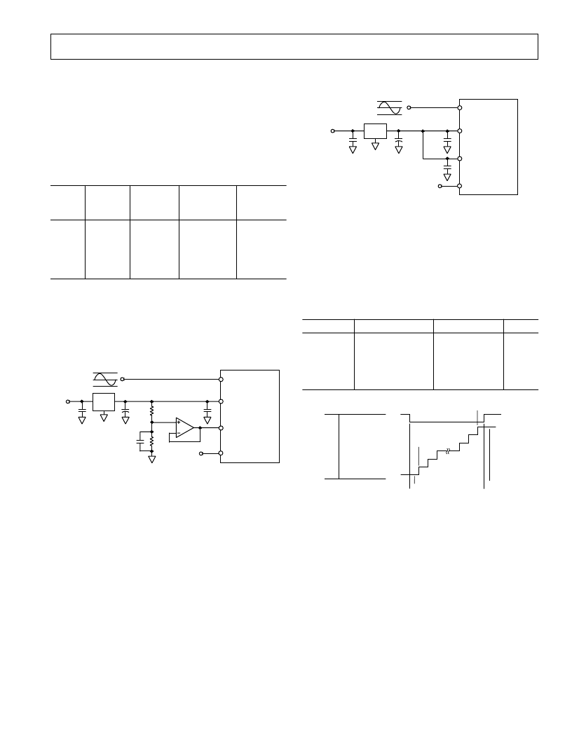
Figure 29. External Reference
Variable Input Span with V
CM
= 2.5 V
Figure 29 shows an example of the AD9225 configured for an
input span of 2
×
VREF centered at 2.5 V. An external 2.5 V
reference drives the VINB pin thus setting the common-mode
voltage at 2.5 V. The input span can be independently set by a
voltage divider consisting of R1 and R2 which generates the
VREF signal. A1 buffers this resistor network and drives
VREF. Choose this op amp based on accuracy requirements. It
is essential that a minimum of a 10
μ
F capacitor in parallel with
a 0.1
μ
F low inductance ceramic capacitor decouple A1’s output
to ground.
Single-Ended Input with 0 to 2
3
VREF Range
Figure 30 shows an example of an external reference driving
both VINB and VREF. In this case, both the common-mode
voltage and input span are directly dependent on the value of
VREF. More specifically, the common-mode voltage is equal to
VREF while the input span is equal to 2
×
VREF. Thus, the
valid input range extends from 0 to 2
×
VREF. For example, if
the REF191, a 2.048 V external reference was selected, the valid
input range extends from 0 to 4.096 V. In this case, 1 LSB of
the AD9225 corresponds to 1 mV. It is essential that a mini-
mum of a 10
μ
F capacitor in parallel with a 0.1
μ
F low inductance
ceramic capacitor decouple the reference output to ground.
2
3
REF
0V
+5V
10
m
F
VINA
VINB
VREF
SENSE
AD9225
+5V
0.1
m
F
VREF
0.1
m
F
0.1
m
F
Figure 30. Input Range = 0 V to 2
×
VREF
DIGITAL INPUTS AND OUTPUTS
Digital Outputs
The AD9225 output data is presented in positive true straight
binary for all input ranges. Table IV indicates the output data
formats for various input ranges regardless of the selected input
range. A twos complement output data format can be created by
inverting the MSB.
Table IV. Output Data Format
I
nput (V)
Condition (V)
Digital Output
OTR
VINA–VINB
VINA–VINB
VINA–VINB
VINA–VINB
VINA–VINB
< – VREF
= – VREF
= 0
= + VREF – 1 LSB
≥
+ VREF
0000 0000 0000
0000 0000 0000
1000 0000 0000
1111 1111 1111
1111 1111 1111
1
0
0
0
1
1111 1111 1111
1111 1111 1111
1111 1111 1110
OTR
–FS
+FS
–FS+1/2 LSB
+FS –1/2 LSB
–FS –1/2 LSB
+FS –1 1/2 LSB
0000 0000 0001
0000 0000 0000
0000 0000 0000
1
0
0
0
0
1
OTR DATA OUTPUTS
Figure 31. Output Data Format
Out Of Range (OTR)
An out-of-range condition exists when the analog input voltage
is beyond the input range of the converter. OTR is a digital out
put that is updated along with the data output corresponding to
the particular sampled analog input voltage. Hence, OTR has
the same pipeline delay (latency) as the digital data. It is LOW
when the analog input voltage is within the analog input range.
It is HIGH when the analog input voltage exceeds the input
range as shown in Figure 32. OTR will remain HIGH until the
analog input returns within the input range and another conver-
sion is completed. By logical ANDing OTR with the MSB and
its complement, overrange high or underrange low conditions
can be detected. Table V is a truth table for the over/underrange
circuit in Figure 33 which uses NAND gates. Systems requiring
programmable gain conditioning of the AD9225 input signal
can immediately detect an out-of-range condition, thus elimi-
nating gain selection iterations. Also, OTR can be used for
digital offset and gain calibration.
相关PDF资料 |
PDF描述 |
|---|---|
| AD9225AR | Complete 12-Bit, 25 MSPS Monolithic A/D Converter |
| AD9225ARS | Complete 12-Bit, 25 MSPS Monolithic A/D Converter |
| AD9226-LQFP-EB | Complete 12-Bit, 65 MSPS ADC Converter |
| AD9226 | Complete 12-Bit, 65 MSPS ADC Converter |
| AD9226-EB | Complete 12-Bit, 65 MSPS ADC Converter |
相关代理商/技术参数 |
参数描述 |
|---|---|
| AD9226 | 制造商:AD 制造商全称:Analog Devices 功能描述:Complete 12-Bit, 65 MSPS ADC Converter |
| AD9226_01 | 制造商:AD 制造商全称:Analog Devices 功能描述:Complete 12-Bit, 65 MSPS ADC Converter |
| AD9226ARS | 功能描述:IC ADC 12BIT 65MSPS 28-SSOP RoHS:否 类别:集成电路 (IC) >> 数据采集 - 模数转换器 系列:- 产品培训模块:Lead (SnPb) Finish for COTS Obsolescence Mitigation Program 标准包装:2,500 系列:- 位数:12 采样率(每秒):3M 数据接口:- 转换器数目:- 功率耗散(最大):- 电压电源:- 工作温度:- 安装类型:表面贴装 封装/外壳:SOT-23-6 供应商设备封装:SOT-23-6 包装:带卷 (TR) 输入数目和类型:- |
| AD9226ARSRL | 功能描述:IC ADC 12BIT 65MSPS 28-SSOP RoHS:否 类别:集成电路 (IC) >> 数据采集 - 模数转换器 系列:- 产品培训模块:Lead (SnPb) Finish for COTS Obsolescence Mitigation Program 标准包装:2,500 系列:- 位数:12 采样率(每秒):3M 数据接口:- 转换器数目:- 功率耗散(最大):- 电压电源:- 工作温度:- 安装类型:表面贴装 封装/外壳:SOT-23-6 供应商设备封装:SOT-23-6 包装:带卷 (TR) 输入数目和类型:- |
| AD9226ARSZ | 功能描述:IC ADC 12BIT 65MSPS 28-SSOP RoHS:是 类别:集成电路 (IC) >> 数据采集 - 模数转换器 系列:- 标准包装:1 系列:- 位数:14 采样率(每秒):83k 数据接口:串行,并联 转换器数目:1 功率耗散(最大):95mW 电压电源:双 ± 工作温度:0°C ~ 70°C 安装类型:通孔 封装/外壳:28-DIP(0.600",15.24mm) 供应商设备封装:28-PDIP 包装:管件 输入数目和类型:1 个单端,双极 |
发布紧急采购,3分钟左右您将得到回复。