- 您现在的位置:买卖IC网 > PDF目录10661 > AD9225ARSZ (Analog Devices Inc)IC ADC 12BIT 25MSPS 28-SSOP PDF资料下载
参数资料
| 型号: | AD9225ARSZ |
| 厂商: | Analog Devices Inc |
| 文件页数: | 4/25页 |
| 文件大小: | 0K |
| 描述: | IC ADC 12BIT 25MSPS 28-SSOP |
| 标准包装: | 1 |
| 位数: | 12 |
| 采样率(每秒): | 25M |
| 数据接口: | 并联 |
| 转换器数目: | 7 |
| 功率耗散(最大): | 373mW |
| 电压电源: | 单电源 |
| 工作温度: | -40°C ~ 85°C |
| 安装类型: | 表面贴装 |
| 封装/外壳: | 28-SSOP(0.209",5.30mm 宽) |
| 供应商设备封装: | 28-SSOP |
| 包装: | 管件 |
| 输入数目和类型: | 2 个单端,双极;1 个差分,单极 |
| 产品目录页面: | 780 (CN2011-ZH PDF) |
–12–
AD9225
Differential modes of operation (ac-coupled or dc-coupled input)
provide the best THD and SFDR performance over a wide fre-
quency range. Differential operation should be considered for the
most demanding spectral based applications (e.g., direct IF-to-
digital conversion). See Figures 12 and 13 and the Differential
Mode of Operation section. Differential input characterization was
performed for this data sheet using the configuration shown in
Figure 13.
Single-ended operation requires that VINA be ac-coupled or dc-
coupled to the input signal source while VINB of the AD9225 be
biased to the appropriate voltage corresponding to a midscale code
transition. Note that signal inversion may be easily accomplished
by transposing VINA and VINB. Most of the single-ended specifi-
cations for the AD9225 are characterized using Figure 21 circuitry
with input spans of 4 V and 2 V as well as VINB = 2.5 V.
Differential operation requires that VINA and VINB be simulta-
neously driven with two equal signals that are in and out of phase
versions of the input signal. Differential operation of the AD9225
offers the following benefits: (1) Signal swings are smaller and,
therefore, linearity requirements placed on the input signal source
may be easier to achieve, (2) Signal swings are smaller and there-
fore may allow the use of op amps which may otherwise have been
constrained by headroom limitations, (3) Differential operation
minimizes even-order harmonic products, and (4) Differential
operation offers noise immunity based on the device’s common-
mode rejection.
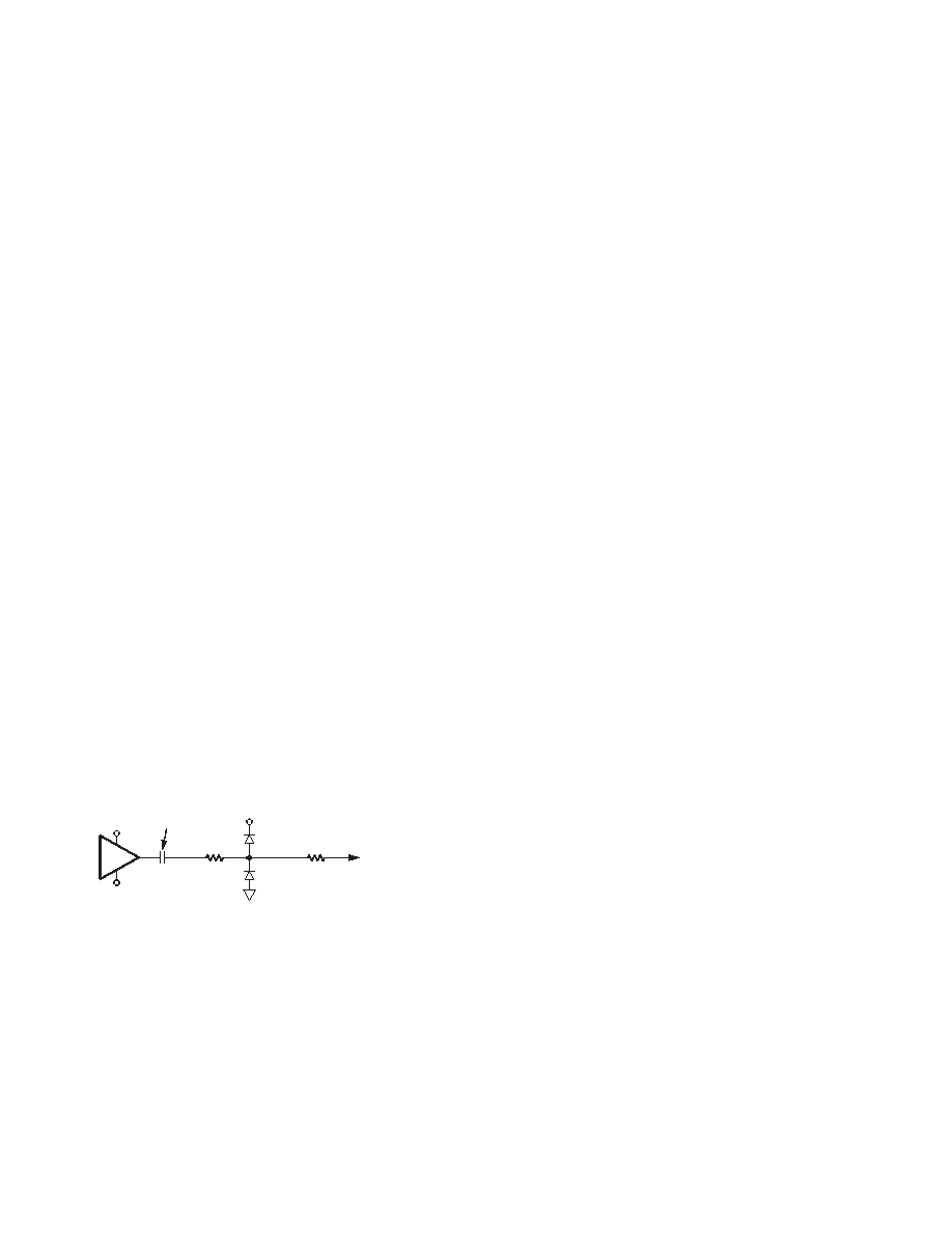
As is typical of most IC devices, exceeding the supply limits will
turn on internal parasitic diodes resulting in transient currents
within the device. Figure 7 shows a simple means of clamping an
ac-coupled or dc-coupled single-ended input with the addition of
two series resistors and two diodes. An optional capacitor is shown
for ac-coupled applications. Note that a larger series resistor could
be used to limit the fault current through D1 and D2 but should
be evaluated since it can cause a degradation in overall perfor-
mance. A similar clamping circuit could also be used for each input
if a differential input signal is being applied. The diodes might
cause nonlinearities in the signal. Careful evaluation should be
performed on the diodes used.
AVDD
AD9225
RS1
30
VCC
VEE
OPTIONAL
AC COUPLING
CAPACITOR
D2
1N4148
D1
1N4148
RS2
20
Figure 7. Simple Clamping Circuit
SINGLE-ENDED MODE OF OPERATION
The AD9225 can be configured for single-ended operation using
dc-coupling or ac-coupling. In either case, the input of the ADC
must be driven from an operational amplifier that will not degrade
the ADC’s performance. Because the ADC operates from a single
supply, it will be necessary to level shift ground based bipolar
signals to comply with its input requirements. Both dc and ac
coupling provide this necessary function, but each method results
in different interface issues that may influence the system design
and performance.
Single-ended operation is often limited by the availability of driving
op amps. Very low distortion op amps that provide great perfor-
mance out to the Nyquist frequency of the converter are hard to
find. Compounding the problem, for dc-coupled, single-ended
applications, is the inability of many high performance amplifiers
to maintain low distortions as their outputs approach their positive
output voltage limit (i.e., 1 dB compression point). For this reason,
it is recommended that applications requiring high performance
dc coupling use the single-ended-to-differential circuit shown in
Figure 12.
DC COUPLING AND INTERFACE ISSUES
Many applications require the analog input signal to be dc-coupled
to the AD9225. An operational amplifier can be configured to
rescale and level shift the input signal so that it is compatible with
the selected input range of the ADC. The input range to the ADC
should be selected on the basis of system performance objectives,
as well as the analog power supply availability since this will place
certain constraints on the op amp selection.
Many of the new high performance op amps are specified for only
±5 V operation and have limited input/output swing capabilities.
The selected input range of the AD9225 should be considered with
the headroom requirements of the particular op amp to prevent
clipping of the signal. Since the output of a dual supply amplifier
can swing below –0.3 V, clamping its output should be considered
in some applications.
In some applications, it may be advantageous to use an op amp
specified for single-supply +5 V operation since it will inherently
limit its output swing to within the power supply rails. Amplifiers
like the AD8041 and AD8011 are useful for this purpose but their
low bandwidths will limit the AD9225’s performance. High perfor-
mance amplifiers, such as the AD9631, AD9632, AD8056, or
AD8055, allow the AD9225 to be configured for larger input spans
which will improve the ADC’s noise performance.
Op amp circuits using a noninverting and inverting topology are
discussed in the next section. Although not shown, the non-
inverting and inverting topologies can be easily configured as part
of an antialiasing filter by using a Sallen-Key or multiple-feedback
topology. An additional R-C network can be inserted between the
op amp output and the AD9225 input to provide a filter pole.
Simple Op Amp Buffer
In the simplest case, the input signal to the AD9225 will already be
biased at levels in accordance with the selected input range. It is
simply necessary to provide an adequately low source impedance
for the VINA and VINB analog pins of the ADC. Figure 8 shows
the recommended configuration a single-ended drive using an op
amp. In this case, the op amp is shown in a noninverting unity gain
configuration driving the VINA pin. The internal reference drives
the VINB pin. Note that the addition of a small series resistor of
30
W to 50 W connected to VINA and VINB will be beneficial in
nearly all cases. Refer to the Analog Input Operation section on a
discussion on resistor selection. Figure 8 shows the proper connec-
tion for a 0 V to 4 V input range. Alternative single-ended ranges
of 0 V to 2
VREF can also be realized with the proper configura-
tion of VREF (refer to the Using the Internal Reference section).
Headroom limitations of the op amp must always be considered.
Rev. C
相关PDF资料 |
PDF描述 |
|---|---|
| VI-B1W-IV-F1 | CONVERTER MOD DC/DC 5.5V 150W |
| AD9225ARZ | IC ADC 12BIT 25MSPS 28-SOIC |
| VE-B1W-IV-F2 | CONVERTER MOD DC/DC 5.5V 150W |
| MAX13430EETB+T | TXRX RS-485 0.5MBPS HALF 10TDFN |
| LTC2247CUH#PBF | IC ADC 14BIT 40MSPS SAMPL 32-QFN |
相关代理商/技术参数 |
参数描述 |
|---|---|
| AD9225ARSZ | 制造商:Analog Devices 功能描述:IC 制造商:Analog Devices 功能描述:IC, ADC, 12BIT, 25MSPS, SSOP-28 |
| AD9225ARSZRL | 功能描述:IC ADC 12BIT 25MSPS 28SSOP RoHS:是 类别:集成电路 (IC) >> 数据采集 - 模数转换器 系列:- 标准包装:1,000 系列:- 位数:12 采样率(每秒):300k 数据接口:并联 转换器数目:1 功率耗散(最大):75mW 电压电源:单电源 工作温度:0°C ~ 70°C 安装类型:表面贴装 封装/外壳:24-SOIC(0.295",7.50mm 宽) 供应商设备封装:24-SOIC 包装:带卷 (TR) 输入数目和类型:1 个单端,单极;1 个单端,双极 |
| AD9225ARZ | 功能描述:IC ADC 12BIT 25MSPS 28-SOIC RoHS:是 类别:集成电路 (IC) >> 数据采集 - 模数转换器 系列:- 标准包装:1 系列:microPOWER™ 位数:8 采样率(每秒):1M 数据接口:串行,SPI? 转换器数目:1 功率耗散(最大):- 电压电源:模拟和数字 工作温度:-40°C ~ 125°C 安装类型:表面贴装 封装/外壳:24-VFQFN 裸露焊盘 供应商设备封装:24-VQFN 裸露焊盘(4x4) 包装:Digi-Reel® 输入数目和类型:8 个单端,单极 产品目录页面:892 (CN2011-ZH PDF) 其它名称:296-25851-6 |
| AD9225ARZRL | 功能描述:IC ADC 12BIT 25MSPS 28SOIC RoHS:是 类别:集成电路 (IC) >> 数据采集 - 模数转换器 系列:- 标准包装:1,000 系列:- 位数:12 采样率(每秒):300k 数据接口:并联 转换器数目:1 功率耗散(最大):75mW 电压电源:单电源 工作温度:0°C ~ 70°C 安装类型:表面贴装 封装/外壳:24-SOIC(0.295",7.50mm 宽) 供应商设备封装:24-SOIC 包装:带卷 (TR) 输入数目和类型:1 个单端,单极;1 个单端,双极 |
| AD9225-EB | 制造商:Analog Devices 功能描述: 制造商:Analog Devices 功能描述:DEV TOOLS, EVAL BD FOR AD9225 - Bulk |
发布紧急采购,3分钟左右您将得到回复。