- 您现在的位置:买卖IC网 > PDF目录17024 > AD9228-65EBZ (Analog Devices Inc)BOARD EVAL FOR AD9228 PDF资料下载
参数资料
| 型号: | AD9228-65EBZ |
| 厂商: | Analog Devices Inc |
| 文件页数: | 26/56页 |
| 文件大小: | 0K |
| 描述: | BOARD EVAL FOR AD9228 |
| 设计资源: | AD9219/28/59/87 Gerber Files |
| 标准包装: | 1 |
| ADC 的数量: | 4 |
| 位数: | 12 |
| 采样率(每秒): | 65M |
| 数据接口: | 串行 |
| 输入范围: | 2 Vpp |
| 在以下条件下的电源(标准): | 119mW @ 65MSPS |
| 工作温度: | -40°C ~ 85°C |
| 已用 IC / 零件: | AD9228 |
| 已供物品: | 板,电源 |
第1页第2页第3页第4页第5页第6页第7页第8页第9页第10页第11页第12页第13页第14页第15页第16页第17页第18页第19页第20页第21页第22页第23页第24页第25页当前第26页第27页第28页第29页第30页第31页第32页第33页第34页第35页第36页第37页第38页第39页第40页第41页第42页第43页第44页第45页第46页第47页第48页第49页第50页第51页第52页第53页第54页第55页第56页
AD9228
Data Sheet
Rev. E | Page 32 of 56
05
72
7-
1
02
NUMBER OF SDIO PINS CONNECTED TOGETHER
V
OH
(V
)
1.715
1.720
1.725
1.730
1.735
1.740
1.745
1.750
1.755
1.760
1.765
1.770
1.775
1.780
1.785
1.790
1.795
1.800
030
20
10
40
50
60
70
80
90
100
Figure 68. SDIO Pin Loading
If the user chooses not to use the SPI, these dual-function pins
serve their secondary functions when the CSB is strapped to
AVDD during device power-up. See the Theory of Operation
section for details on which pin-strappable functions are
supported on the SPI pins.
For users who wish to operate the ADC without using the
SPI, remove any connections from the CSB, SCLK/DTP, and
SDIO/ODM pins. By disconnecting these pins from the control
bus, the ADC can function in its most basic operation. Each
of these pins has an internal termination that floats to its
respective level.
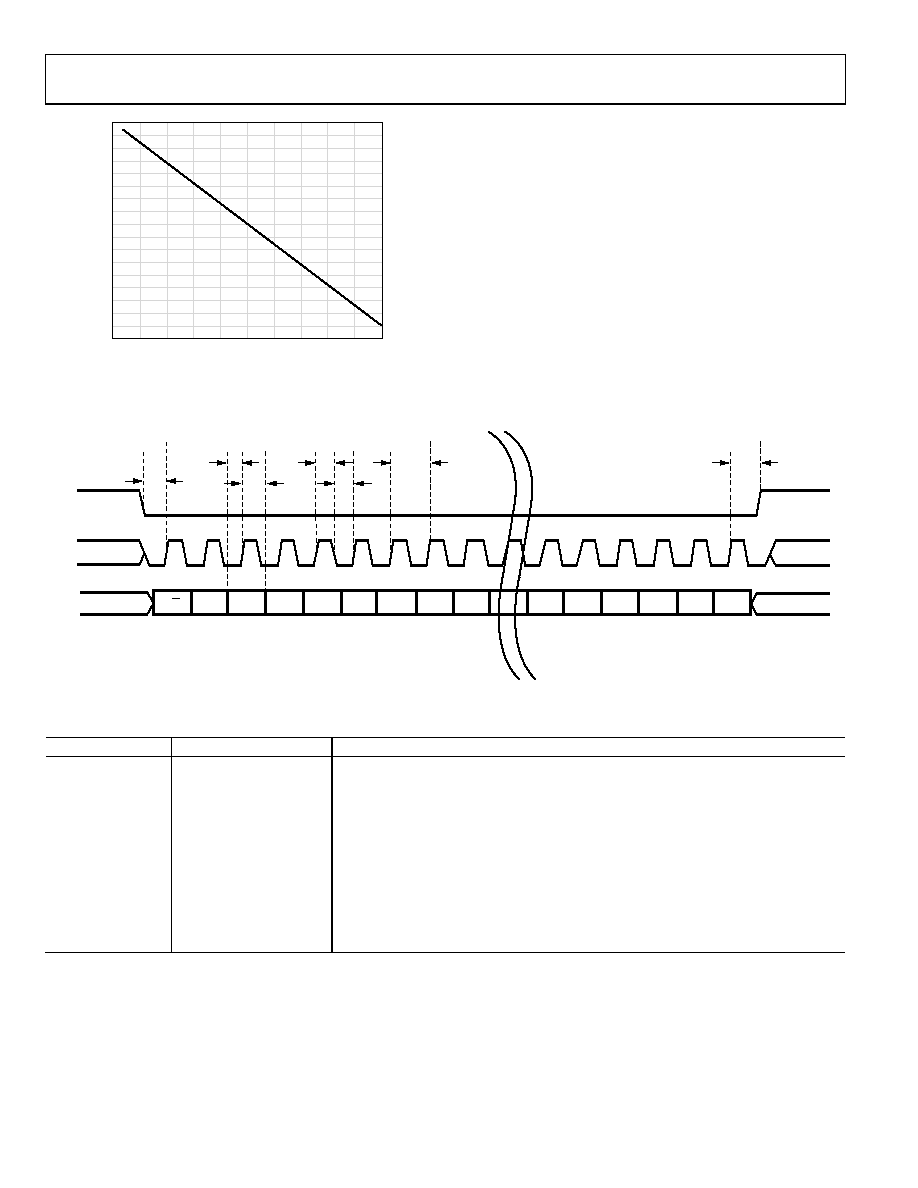
DON’T CARE
SDIO
SCLK
CSB
tS
tDH
tHI
tCLK
tLO
tDS
tH
R/W
W1
W0
A12
A11
A10
A9
A8
A7
D5
D4
D3
D2
D1
D0
05
727-
012
Figure 69. Serial Timing Details
Table 15. Serial Timing Definitions
Parameter
Timing (Minimum, ns)
Description
tDS
5
Setup time between the data and the rising edge of SCLK
tDH
2
Hold time between the data and the rising edge of SCLK
tCLK
40
Period of the clock
tS
5
Setup time between CSB and SCLK
tH
2
Hold time between CSB and SCLK
tHI
16
Minimum period that SCLK should be in a logic high state
tLO
16
Minimum period that SCLK should be in a logic low state
tEN_SDIO
10
Minimum time for the SDIO pin to switch from an input to an output relative to the SCLK
falling edge (not shown in Figure 69)
tDIS_SDIO
10
Minimum time for the SDIO pin to switch from an output to an input relative to the SCLK
rising edge (not shown in Figure 69)
相关PDF资料 |
PDF描述 |
|---|---|
| GSM10DRST | CONN EDGECARD 20POS DIP .156 SLD |
| STD21W-A | WIRE & CABLE MARKERS |
| DK-SI-5SGXEA7N | KIT DEV STRATIX V FPGA 5SGXEA7 |
| AD676-EB | BOARD EVAL SAMPLING ADC AD676 |
| AD9211-200EBZ | BOARD EVAL FOR AD9211-200 |
相关代理商/技术参数 |
参数描述 |
|---|---|
| AD9228ABCPZ-40 | 功能描述:IC ADC 12BIT SPI/SRL 40M 48LFCSP RoHS:是 类别:集成电路 (IC) >> 数据采集 - 模数转换器 系列:- 其它有关文件:TSA1204 View All Specifications 标准包装:1 系列:- 位数:12 采样率(每秒):20M 数据接口:并联 转换器数目:2 功率耗散(最大):155mW 电压电源:模拟和数字 工作温度:-40°C ~ 85°C 安装类型:表面贴装 封装/外壳:48-TQFP 供应商设备封装:48-TQFP(7x7) 包装:Digi-Reel® 输入数目和类型:4 个单端,单极;2 个差分,单极 产品目录页面:1156 (CN2011-ZH PDF) 其它名称:497-5435-6 |
| AD9228ABCPZ-65 | 功能描述:IC ADC 12BIT SPI/SRL 65M 48LFCSP RoHS:是 类别:集成电路 (IC) >> 数据采集 - 模数转换器 系列:- 其它有关文件:TSA1204 View All Specifications 标准包装:1 系列:- 位数:12 采样率(每秒):20M 数据接口:并联 转换器数目:2 功率耗散(最大):155mW 电压电源:模拟和数字 工作温度:-40°C ~ 85°C 安装类型:表面贴装 封装/外壳:48-TQFP 供应商设备封装:48-TQFP(7x7) 包装:Digi-Reel® 输入数目和类型:4 个单端,单极;2 个差分,单极 产品目录页面:1156 (CN2011-ZH PDF) 其它名称:497-5435-6 |
| AD9228ABCPZRL7-40 | 功能描述:IC ADC 12BIT SPI/SRL 40M 48LFCSP RoHS:是 类别:集成电路 (IC) >> 数据采集 - 模数转换器 系列:- 标准包装:1 系列:- 位数:14 采样率(每秒):83k 数据接口:串行,并联 转换器数目:1 功率耗散(最大):95mW 电压电源:双 ± 工作温度:0°C ~ 70°C 安装类型:通孔 封装/外壳:28-DIP(0.600",15.24mm) 供应商设备封装:28-PDIP 包装:管件 输入数目和类型:1 个单端,双极 |
| AD9228ABCPZRL7-65 | 功能描述:IC ADC 12BIT SPI/SRL 65M 48LFCSP RoHS:是 类别:集成电路 (IC) >> 数据采集 - 模数转换器 系列:- 标准包装:1 系列:- 位数:14 采样率(每秒):83k 数据接口:串行,并联 转换器数目:1 功率耗散(最大):95mW 电压电源:双 ± 工作温度:0°C ~ 70°C 安装类型:通孔 封装/外壳:28-DIP(0.600",15.24mm) 供应商设备封装:28-PDIP 包装:管件 输入数目和类型:1 个单端,双极 |
| AD9228BCPZ-40 | 制造商:Analog Devices 功能描述:ADC Quad Pipelined 40Msps 12-bit Serial 48-Pin LFCSP EP 制造商:Analog Devices 功能描述:IC SM 12-BIT ADC QUAD WAFFLE125 制造商:Analog Devices 功能描述:IC 12BIT ADC QUAD 40MSPS LFCSP48 制造商:Analog Devices 功能描述:IC, 12BIT ADC, QUAD 40MSPS, LFCSP48 |
发布紧急采购,3分钟左右您将得到回复。