- 您现在的位置:买卖IC网 > PDF目录10199 > AD9231BCPZRL7-40 (Analog Devices Inc)IC ADC 12BIT 40MSPS 64LFCSP PDF资料下载
参数资料
| 型号: | AD9231BCPZRL7-40 |
| 厂商: | Analog Devices Inc |
| 文件页数: | 17/36页 |
| 文件大小: | 0K |
| 描述: | IC ADC 12BIT 40MSPS 64LFCSP |
| 标准包装: | 750 |
| 位数: | 12 |
| 采样率(每秒): | 40M |
| 数据接口: | 串行,SPI? |
| 转换器数目: | 2 |
| 功率耗散(最大): | 103mW |
| 电压电源: | 模拟和数字 |
| 工作温度: | -40°C ~ 85°C |
| 安装类型: | 表面贴装 |
| 封装/外壳: | 64-VFQFN 裸露焊盘,CSP |
| 供应商设备封装: | 64-LFCSP-VQ(9x9) |
| 包装: | 带卷 (TR) |
| 输入数目和类型: | 4 个单端,单极;2 个差分,单极 |
第1页第2页第3页第4页第5页第6页第7页第8页第9页第10页第11页第12页第13页第14页第15页第16页当前第17页第18页第19页第20页第21页第22页第23页第24页第25页第26页第27页第28页第29页第30页第31页第32页第33页第34页第35页第36页
AD9231
Rev. A | Page 24 of 36
If a low jitter clock source is not available, another option is to
ac couple a differential PECL signal to the sample clock input
excellent jitter performance.
100
0.1F
240
50k
CLK–
CLK+
CLOCK
INPUT
CLOCK
INPUT
ADC
AD951x
PECL DRIVER
0
812
1-
01
9
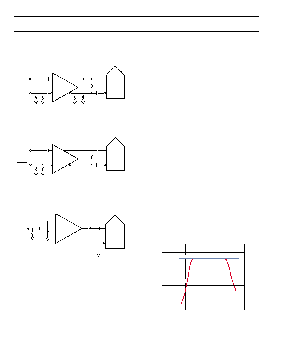
Figure 52. Differential PECL Sample Clock (Up to 625 MHz)
A third option is to ac couple a differential LVDS signal to the
sample clock input pins, as shown in Figure 53. The AD9510/
clock drivers offer excellent jitter performance.
100
0.1F
50k
CLK–
CLK+
ADC
CLOCK
INPUT
CLOCK
INPUT
AD951x
LVDS DRIVER
0
812
1-
020
Figure 53. Differential LVDS Sample Clock (Up to 625 MHz)
In some applications, it may be acceptable to drive the sample
clock inputs with a single-ended 1.8 V CMOS signal. In such
applications, drive the CLK+ pin directly from a CMOS gate, and
bypass the CLK pin to ground with a 0.1 μF capacitor (see
OPTIONAL
100
0.1F
501
150 RESISTOR IS OPTIONAL.
CLK–
CLK+
ADC
VCC
1k
CLOCK
INPUT
AD951x
CMOS DRIVER
08
12
1-
02
1
Figure 54. Single-Ended 1.8 V CMOS Input Clock (Up to 200 MHz)
Input Clock Divider
The AD9231 contains an input clock divider with the ability
to divide the input clock by integer values between 1 and 8.
Optimum performance is obtained by enabling the internal
duty cycle stabilizer (DCS) when using divide ratios other
than 1, 2, or 4.
The AD9231 clock divider can be synchronized using the
external SYNC input. Bit 1 and Bit 2 of Register 0x100 allow
the clock divider to be resynchronized on every SYNC signal
or only on the first SYNC signal after the register is written. A
valid SYNC causes the clock divider to reset to its initial state.
This synchronization feature allows multiple parts to have
their clock dividers aligned to guarantee simultaneous input
sampling.
Clock Duty Cycle
Typical high speed ADCs use both clock edges to generate
a variety of internal timing signals and, as a result, may be
sensitive to clock duty cycle. Commonly, a ±5% tolerance is
required on the clock duty cycle to maintain dynamic
performance characteristics.
The AD9231 contains a duty cycle stabilizer (DCS) that retimes
the nonsampling (falling) edge, providing an internal clock
signal with a nominal 50% duty cycle. This allows the user to
provide a wide range of clock input duty cycles without affecting
the performance of the AD9231. Noise and distortion perform-
ance are nearly flat for a wide range of duty cycles with the DCS
on, as shown in Figure 55.
Jitter in the rising edge of the input is still of concern and is not
easily reduced by the internal stabilization circuit. The duty
cycle control loop does not function for clock rates less than
20 MHz nominally. The loop has a time constant associated
with it that must be considered in applications in which the
clock rate can change dynamically. A wait time of 1.5 μs to 5 μs
is required after a dynamic clock frequency increase or decrease
before the DCS loop is relocked to the input signal.
40
45
50
55
60
65
70
75
80
10
20
30
40
50
60
70
80
S
NR
(
d
B
F
S
)
POSITIVE DUTY CYCLE (%)
DCS OFF
DCS ON
08
12
1-
07
8
Figure 55. SNR vs. DCS On/Off
相关PDF资料 |
PDF描述 |
|---|---|
| CS6422-CS | IC CODEC SPKRPHONE 2CH 20-SOIC |
| AD9649BCPZRL7-20 | IC ADC 14BIT 20MSPS 32LFCSP |
| CXS3102A2027P | CONN RCPT 14POS PNL MNT PIN |
| SP3239ECA-L/TR | IC TXRX RS232 INTELLIGENT 28SSOP |
| MS27467T11F98PD | CONN PLUG 6POS STRAIGHT W/PINS |
相关代理商/技术参数 |
参数描述 |
|---|---|
| AD9231BCPZRL7-65 | 功能描述:IC ADC 12BIT 65MSPS 64LFCSP RoHS:是 类别:集成电路 (IC) >> 数据采集 - 模数转换器 系列:- 标准包装:1 系列:- 位数:14 采样率(每秒):83k 数据接口:串行,并联 转换器数目:1 功率耗散(最大):95mW 电压电源:双 ± 工作温度:0°C ~ 70°C 安装类型:通孔 封装/外壳:28-DIP(0.600",15.24mm) 供应商设备封装:28-PDIP 包装:管件 输入数目和类型:1 个单端,双极 |
| AD9231BCPZRL7-80 | 功能描述:IC ADC 12BIT 80MSPS 64LFCSP RoHS:是 类别:集成电路 (IC) >> 数据采集 - 模数转换器 系列:- 标准包装:1 系列:- 位数:14 采样率(每秒):83k 数据接口:串行,并联 转换器数目:1 功率耗散(最大):95mW 电压电源:双 ± 工作温度:0°C ~ 70°C 安装类型:通孔 封装/外壳:28-DIP(0.600",15.24mm) 供应商设备封装:28-PDIP 包装:管件 输入数目和类型:1 个单端,双极 |
| AD9233 | 制造商:AD 制造商全称:Analog Devices 功能描述:12-Bit, 80 MSPS/105 MSPS/125 MSPS, 1.8 V Analog-to-Digital Converter |
| AD9233-105EB | 制造商:AD 制造商全称:Analog Devices 功能描述:12-Bit, 80 MSPS/105 MSPS/125 MSPS, 1.8 V Analog-to-Digital Converter |
| AD9233-105EBZ | 制造商:Analog Devices 功能描述: |
发布紧急采购,3分钟左右您将得到回复。