- 您现在的位置:买卖IC网 > PDF目录10533 > AD9235BCPZ-65 (Analog Devices Inc)IC ADC 12BIT 65MSPS 32-LFCSP PDF资料下载
参数资料
| 型号: | AD9235BCPZ-65 |
| 厂商: | Analog Devices Inc |
| 文件页数: | 9/40页 |
| 文件大小: | 0K |
| 描述: | IC ADC 12BIT 65MSPS 32-LFCSP |
| 标准包装: | 1 |
| 位数: | 12 |
| 采样率(每秒): | 65M |
| 数据接口: | 并联 |
| 转换器数目: | 3 |
| 功率耗散(最大): | 300mW |
| 电压电源: | 单电源 |
| 工作温度: | -40°C ~ 85°C |
| 安装类型: | 表面贴装 |
| 封装/外壳: | 32-VFQFN 裸露焊盘,CSP |
| 供应商设备封装: | 32-LFCSP-VQ(5x5) |
| 包装: | 托盘 |
| 输入数目和类型: | 2 个单端,单极;1 个差分,单极 |
第1页第2页第3页第4页第5页第6页第7页第8页当前第9页第10页第11页第12页第13页第14页第15页第16页第17页第18页第19页第20页第21页第22页第23页第24页第25页第26页第27页第28页第29页第30页第31页第32页第33页第34页第35页第36页第37页第38页第39页第40页
Data Sheet
AD9235
Rev. D | Page 17 of 40
High speed, high resolution ADCs are sensitive to the quality of
the clock input. The degradation in SNR at a given full-scale
input frequency (fINPUT) due only to aperture jitter (tJ) can be
calculated by
SNR Degradation = 20 × log10[2π × fINPUT × tJ]
In the equation, the rms aperture jitter, tJ, represents the root-
sum square of all jitter sources, which include the clock input,
analog input signal, and ADC aperture jitter specification.
Undersampling applications are particularly sensitive to jitter.
The clock input should be treated as an analog signal in cases
where aperture jitter may affect the dynamic range of the
AD9235. Power supplies for clock drivers should be separated
from the ADC output driver supplies to avoid modulating the
clock signal with digital noise. Low jitter, crystal-controlled
oscillators make the best clock sources. If the clock is generated
from another type of source (by gating, dividing, or other
methods), it should be retimed by the original clock at the last
step.
POWER DISSIPATION AND STANDBY MODE
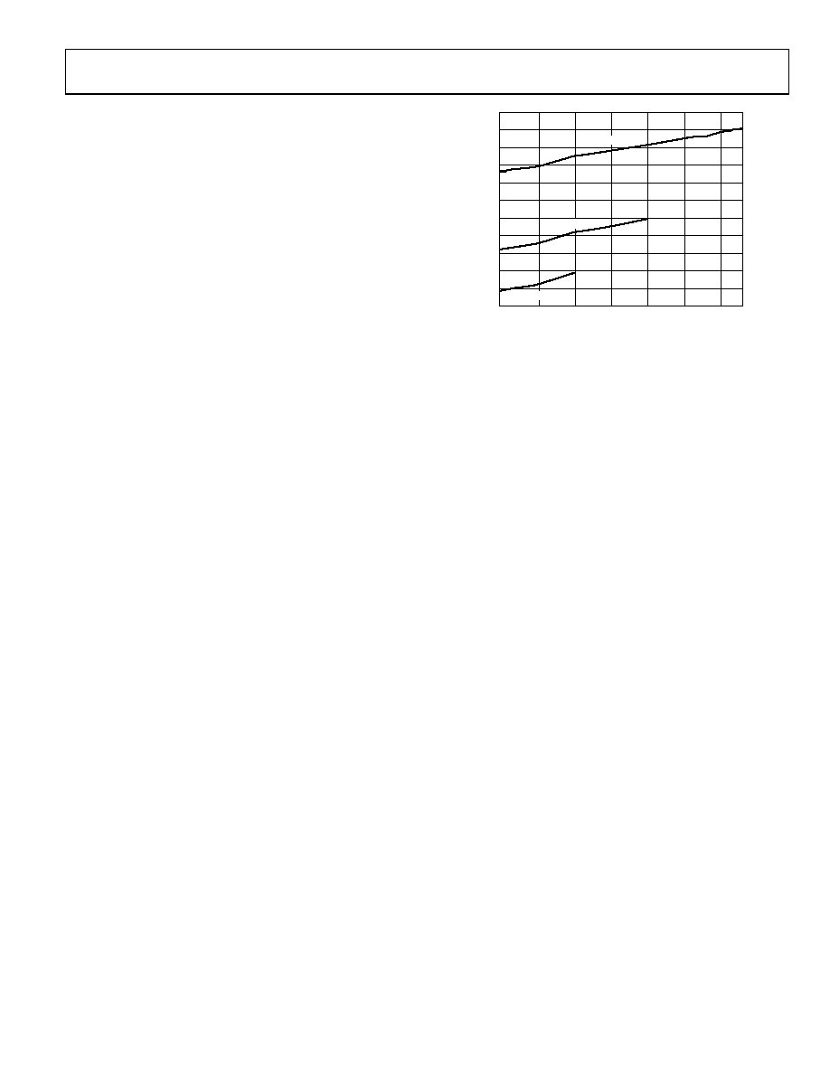
As shown in Figure 38, the power dissipated by the AD9235 is
proportional to its sample rate. The digital power dissipation
does not vary substantially between the three speed grades
because it is determined primarily by the strength of the digital
drivers and the load on each output bit. The maximum DRVDD
current can be calculated as
IDRVDD = VDRVDD × CLOAD × fCLK × N
where N is the number of output bits, 12 in the case of the
AD9235. This maximum current occurs when every output bit
switches on every clock cycle, i.e., a full-scale square wave at the
Nyquist frequency, fCLK/2. In practice, the DRVDD current is
established by the average number of output bits switching,
which is determined by the encode rate and the characteristics
of the analog input signal.
02461-038
SAMPLE RATE (MSPS)
60
0
10
20
30
40
50
TOTAL
POWER
(mW)
325
300
275
250
225
200
175
150
125
100
75
50
AD9235-20
AD9235-40
AD9235-65
Figure 38. Total Power vs. Sample Rate with fIN = 10 MHz
For the AD9235-20 speed grade, the digital power consumption
can represent as much as 10% of the total dissipation. Digital
power consumption can be minimized by reducing the capaci-
tive load presented to the output drivers. The data in Figure 38
was taken with a 5 pF load on each output driver.
The analog circuitry is optimally biased so that each speed
grade provides excellent performance while affording reduced
power consumption. Each speed grade dissipates a baseline
power at low sample rates that increases linearly with the clock
frequency.
By asserting the PDWN pin high, the AD9235 is placed in
standby mode. In this state, the ADC typically dissipates 1 mW
if the CLK and analog inputs are static. During standby, the
output drivers are placed in a high impedance state. Reasserting
the PDWN pin low returns the AD9235 into its normal
operational mode.
Low power dissipation in standby mode is achieved by shutting
down the reference, reference buffer, and biasing networks. The
decoupling capacitors on REFT and REFB are discharged when
entering standby mode and then must be recharged when
returning to normal operation. As a result, the wake-up time is
related to the time spent in standby mode, and shorter standby
cycles result in proportionally shorter wake-up times. With the
recommended 0.1 F and 10 F decoupling capacitors on REFT
and REFB, it takes approximately 1 sec to fully discharge the
reference buffer decoupling capacitors and 3 ms to restore full
operation.
相关PDF资料 |
PDF描述 |
|---|---|
| MS3102A22-15S | CONN RCPT 6POS BOX MNT W/SCKT |
| VE-J40-MY-F1 | CONVERTER MOD DC/DC 5V 50W |
| VE-J3Y-MX-F4 | CONVERTER MOD DC/DC 3.3V 49.5W |
| VE-J3X-MY-F2 | CONVERTER MOD DC/DC 5.2V 50W |
| MS3100A18-16S | CONN RCPT 1POS WALL MNT W/SCKT |
相关代理商/技术参数 |
参数描述 |
|---|---|
| AD9235BCPZRL7-20 | 功能描述:IC ADC 12BIT SGL 20MSPS 32LFCSP RoHS:是 类别:集成电路 (IC) >> 数据采集 - 模数转换器 系列:- 标准包装:1,000 系列:- 位数:16 采样率(每秒):45k 数据接口:串行 转换器数目:2 功率耗散(最大):315mW 电压电源:模拟和数字 工作温度:0°C ~ 70°C 安装类型:表面贴装 封装/外壳:28-SOIC(0.295",7.50mm 宽) 供应商设备封装:28-SOIC W 包装:带卷 (TR) 输入数目和类型:2 个单端,单极 |
| AD9235BCPZRL7-40 | 功能描述:IC ADC 12BIT SGL 40MSPS 32LFCSP RoHS:是 类别:集成电路 (IC) >> 数据采集 - 模数转换器 系列:- 标准包装:1,000 系列:- 位数:12 采样率(每秒):300k 数据接口:并联 转换器数目:1 功率耗散(最大):75mW 电压电源:单电源 工作温度:0°C ~ 70°C 安装类型:表面贴装 封装/外壳:24-SOIC(0.295",7.50mm 宽) 供应商设备封装:24-SOIC 包装:带卷 (TR) 输入数目和类型:1 个单端,单极;1 个单端,双极 |
| AD9235BCPZRL7-65 | 功能描述:IC ADC 12BIT SGL 65MSPS 32LFCSP RoHS:是 类别:集成电路 (IC) >> 数据采集 - 模数转换器 系列:- 标准包装:1,000 系列:- 位数:12 采样率(每秒):300k 数据接口:并联 转换器数目:1 功率耗散(最大):75mW 电压电源:单电源 工作温度:0°C ~ 70°C 安装类型:表面贴装 封装/外壳:24-SOIC(0.295",7.50mm 宽) 供应商设备封装:24-SOIC 包装:带卷 (TR) 输入数目和类型:1 个单端,单极;1 个单端,双极 |
| AD9235BRU-20 | 功能描述:IC ADC 12BIT 20MSPS 28-TSSOP RoHS:否 类别:集成电路 (IC) >> 数据采集 - 模数转换器 系列:- 产品培训模块:Lead (SnPb) Finish for COTS Obsolescence Mitigation Program 标准包装:2,500 系列:- 位数:12 采样率(每秒):3M 数据接口:- 转换器数目:- 功率耗散(最大):- 电压电源:- 工作温度:- 安装类型:表面贴装 封装/外壳:SOT-23-6 供应商设备封装:SOT-23-6 包装:带卷 (TR) 输入数目和类型:- |
| AD9235BRU-20Z | 制造商:Analog Devices 功能描述:ADC 3V 12BIT 20MSPS 0.8LSB 制造商:Analog Devices 功能描述:ADC, 3V, 12BIT, 20MSPS, 0.8LSB, 28TSSOP; Resolution (Bits):12bit; Sampling Rate:20MSPS; Supply Voltage Type:Single; Supply Voltage Min:2.7V; Supply Voltage Max:3.6V; Supply Current:30mA; Digital IC Case Style:TSSOP; No. of Pins:28; ;RoHS Compliant: Yes |
发布紧急采购,3分钟左右您将得到回复。