参数资料
| 型号: | AD9235BRU-65 |
| 厂商: | Analog Devices Inc |
| 文件页数: | 10/40页 |
| 文件大小: | 0K |
| 描述: | IC ADC 12BIT 65MSPS 28-TSSOP |
| 产品变化通告: | Product Discontinuance 27/Oct/2011 |
| 标准包装: | 1 |
| 位数: | 12 |
| 采样率(每秒): | 65M |
| 数据接口: | 并联 |
| 转换器数目: | 3 |
| 功率耗散(最大): | 300mW |
| 电压电源: | 单电源 |
| 工作温度: | -40°C ~ 85°C |
| 安装类型: | 表面贴装 |
| 封装/外壳: | 28-TSSOP(0.173",4.40mm 宽) |
| 供应商设备封装: | 28-TSSOP |
| 包装: | 管件 |
| 输入数目和类型: | 2 个单端,单极;1 个差分,单极 |
第1页第2页第3页第4页第5页第6页第7页第8页第9页当前第10页第11页第12页第13页第14页第15页第16页第17页第18页第19页第20页第21页第22页第23页第24页第25页第26页第27页第28页第29页第30页第31页第32页第33页第34页第35页第36页第37页第38页第39页第40页
AD9235
Data Sheet
Rev. D | Page 18 of 40
Table 7. Reference Configuration Summary
Selected Mode
SENSE Voltage
Internal Switch Position
Resulting VREF (V)
Resulting Differential Span (V p-p)
External Reference
AVDD
N/A
2 × External Reference
Internal Fixed Reference
VREF
SENSE
0.5
1.0
Programmable Reference
0.2 V to VREF
SENSE
0.5 × (1 + R2/R1)
2 × VREF (See Figure 40)
Internal Fixed Reference
AGND to 0.2 V
Internal Divider
1.0
2.0
DIGITAL OUTPUTS
The AD9235 output drivers can be configured to interface with
2.5 V or 3.3 V logic families by matching DRVDD to the digital
supply of the interfaced logic. The output drivers are sized to
provide sufficient output current to drive a wide variety of logic
families. However, large drive currents tend to cause current
glitches on the supplies that may affect converter performance.
Applications requiring the ADC to drive large capacitive loads
or large fan-outs may require external buffers or latches.
As detailed in Table 8, the data format can be selected for either
offset binary or twos complement.
Timing
The AD9235 provides latched data outputs with a pipeline delay
of seven clock cycles. Data outputs are available one propaga-
tion delay (tPD) after the rising edge of the clock signal. Refer to
Figure 2 for a detailed timing diagram.
The length of the output data lines and loads placed on them
should be minimized to reduce transients within the AD9235;
these transients can detract from the converter’s dynamic
performance.
The lowest typical conversion rate of the AD9235 is 1 MSPS. At
clock rates below 1 MSPS, dynamic performance may degrade.
VOLTAGE REFERENCE
A stable and accurate 0.5 V voltage reference is built into the
AD9235. The input range can be adjusted by varying the refer-
ence voltage applied to the AD9235, using either the internal
reference or an externally applied reference voltage. The input
span of the ADC tracks reference voltage changes linearly.
If the ADC is being driven differentially through a transformer,
the reference voltage can be used to bias the center tap
(common-mode voltage).
Internal Reference Connection
A comparator within the AD9235 detects the potential at the
SENSE pin and configures the reference into one of four possi-
ble states, which are summarized in Table 7. If SENSE is
grounded, the reference amplifier switch is connected to the
internal resistor divider (see Figure 39), setting VREF to 1 V.
Connecting the SENSE pin to VREF switches the reference
amplifier output to the SENSE pin, completing the loop and
providing a 0.5 V reference output. If a resistor divider is
connected as shown in Figure 40, the switch is again set to the
SENSE pin. This puts the reference amplifier in a noninverting
mode with the VREF output defined as
VREF = 0.5 × (1 + R2/R1)
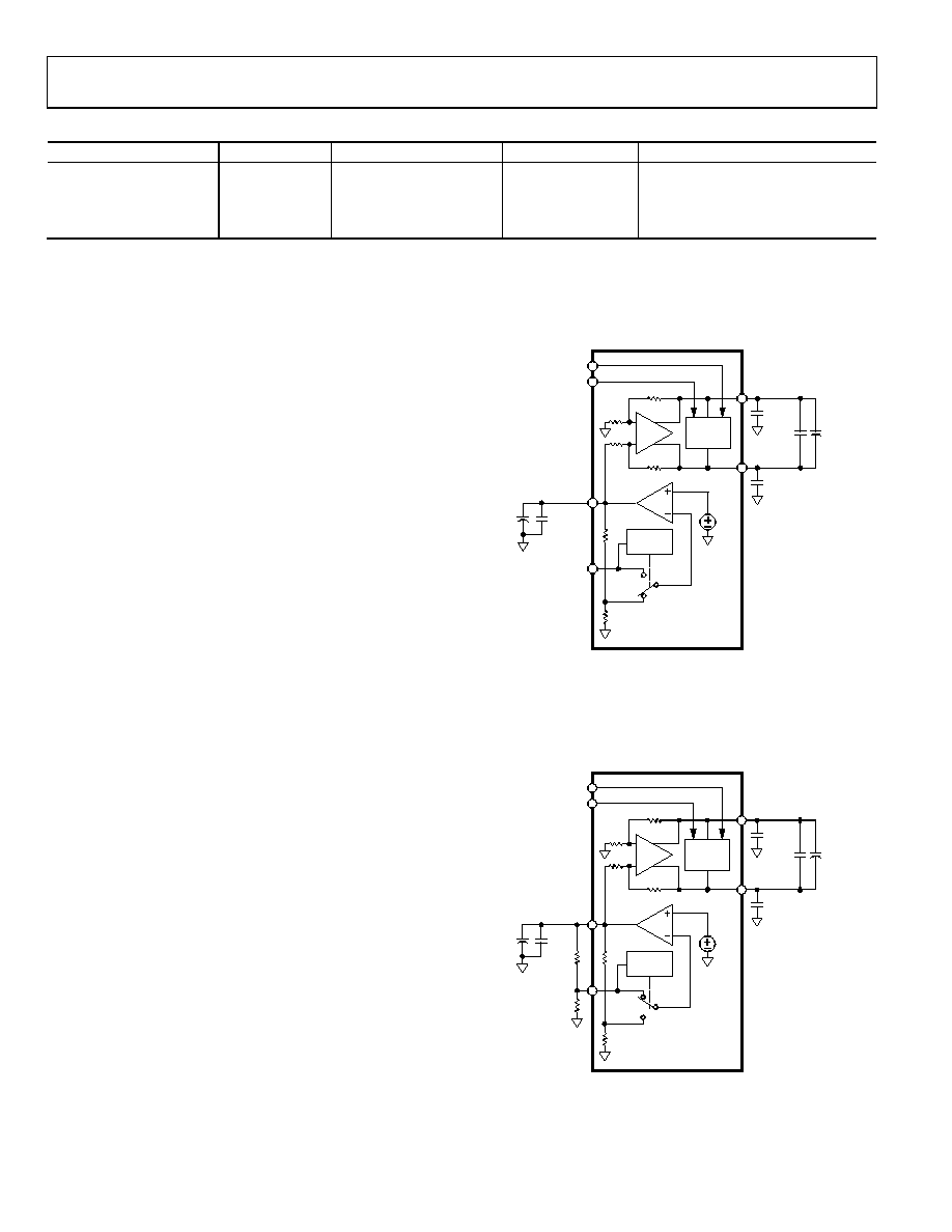
ADC
CORE
SELECT
LOGIC
AD9235
VIN–
VREF
SENSE
VIN+
REFB
REFT
10
F
0.1
F
0.1
F
10
F
0.1
F
0.1
F
0.5V
02461-039
+
Figure 39. Internal Reference Configuration
In all reference configurations, REFT and REFB drive the A/D
conversion core and establish its input span. The input range of
the ADC always equals twice the voltage at the reference pin for
either an internal or an external reference.
02461-040
SENSE
ADC
CORE
SELECT
LOGIC
AD9235
VREF
VIN–
VIN+
REFB
REFT
10
F
0.1
F
0.1
F
10
F
0.1
F
0.1
F
0.5V
R2
R1
+
Figure 40. Programmable Reference Configuration
相关PDF资料 |
PDF描述 |
|---|---|
| MS27656E13A35PB | CONN RCPT 22POS WALL MNT W/PINS |
| MS27467E21F16SB | CONN PLUG 16POS STRAIGHT W/SCKT |
| MS27484T10F35SA | CONN PLUG 13POS STRAIGHT W/SCKT |
| MS3108E16S-5S | CONN PLUG 3POS RT ANG W/SCKT |
| MS27497E22F21SA | CONN RCPT 21POS WALL MNT W/SCKT |
相关代理商/技术参数 |
参数描述 |
|---|---|
| AD9235BRURL7-20 | 功能描述:IC ADC 12BIT SGL 20MSPS 28TSSOP RoHS:否 类别:集成电路 (IC) >> 数据采集 - 模数转换器 系列:- 产品培训模块:Lead (SnPb) Finish for COTS Obsolescence Mitigation Program 标准包装:2,500 系列:- 位数:12 采样率(每秒):3M 数据接口:- 转换器数目:- 功率耗散(最大):- 电压电源:- 工作温度:- 安装类型:表面贴装 封装/外壳:SOT-23-6 供应商设备封装:SOT-23-6 包装:带卷 (TR) 输入数目和类型:- |
| AD9235BRURL7-40 | 功能描述:IC ADC 12BIT SGL 40MSPS 28TSSOP RoHS:否 类别:集成电路 (IC) >> 数据采集 - 模数转换器 系列:- 产品培训模块:Lead (SnPb) Finish for COTS Obsolescence Mitigation Program 标准包装:2,500 系列:- 位数:12 采样率(每秒):3M 数据接口:- 转换器数目:- 功率耗散(最大):- 电压电源:- 工作温度:- 安装类型:表面贴装 封装/外壳:SOT-23-6 供应商设备封装:SOT-23-6 包装:带卷 (TR) 输入数目和类型:- |
| AD9235BRURL7-65 | 功能描述:IC ADC 12BIT 65MSPS 28-TSSOP RoHS:否 类别:集成电路 (IC) >> 数据采集 - 模数转换器 系列:- 产品培训模块:Lead (SnPb) Finish for COTS Obsolescence Mitigation Program 标准包装:2,500 系列:- 位数:12 采样率(每秒):3M 数据接口:- 转换器数目:- 功率耗散(最大):- 电压电源:- 工作温度:- 安装类型:表面贴装 封装/外壳:SOT-23-6 供应商设备封装:SOT-23-6 包装:带卷 (TR) 输入数目和类型:- |
| AD9235BRUZ-20 | 功能描述:IC ADC 12BIT 20MSPS 28-TSSOP RoHS:是 类别:集成电路 (IC) >> 数据采集 - 模数转换器 系列:- 标准包装:1 系列:microPOWER™ 位数:8 采样率(每秒):1M 数据接口:串行,SPI? 转换器数目:1 功率耗散(最大):- 电压电源:模拟和数字 工作温度:-40°C ~ 125°C 安装类型:表面贴装 封装/外壳:24-VFQFN 裸露焊盘 供应商设备封装:24-VQFN 裸露焊盘(4x4) 包装:Digi-Reel® 输入数目和类型:8 个单端,单极 产品目录页面:892 (CN2011-ZH PDF) 其它名称:296-25851-6 |
| AD9235BRUZ-20 | 制造商:Analog Devices 功能描述:IC, ADC, 12BIT, 20MSPS, TSSOP-28 |
发布紧急采购,3分钟左右您将得到回复。