- 您现在的位置:买卖IC网 > PDF目录10155 > AD9236BCPZRL7-80 (Analog Devices Inc)IC ADC 12BIT 80MSPS 32LFCSP PDF资料下载
参数资料
| 型号: | AD9236BCPZRL7-80 |
| 厂商: | Analog Devices Inc |
| 文件页数: | 10/36页 |
| 文件大小: | 0K |
| 描述: | IC ADC 12BIT 80MSPS 32LFCSP |
| 标准包装: | 1,500 |
| 位数: | 12 |
| 采样率(每秒): | 80M |
| 数据接口: | 并联 |
| 转换器数目: | 2 |
| 功率耗散(最大): | 366mW |
| 电压电源: | 模拟和数字 |
| 工作温度: | -40°C ~ 85°C |
| 安装类型: | 表面贴装 |
| 封装/外壳: | 32-VFQFN 裸露焊盘,CSP |
| 供应商设备封装: | 32-LFCSP-VQ(5x5) |
| 包装: | 带卷 (TR) |
| 输入数目和类型: | 2 个单端,单极;1 个差分,单极 |
第1页第2页第3页第4页第5页第6页第7页第8页第9页当前第10页第11页第12页第13页第14页第15页第16页第17页第18页第19页第20页第21页第22页第23页第24页第25页第26页第27页第28页第29页第30页第31页第32页第33页第34页第35页第36页
AD9236
Data Sheet
Rev. C | Page 18 of 36
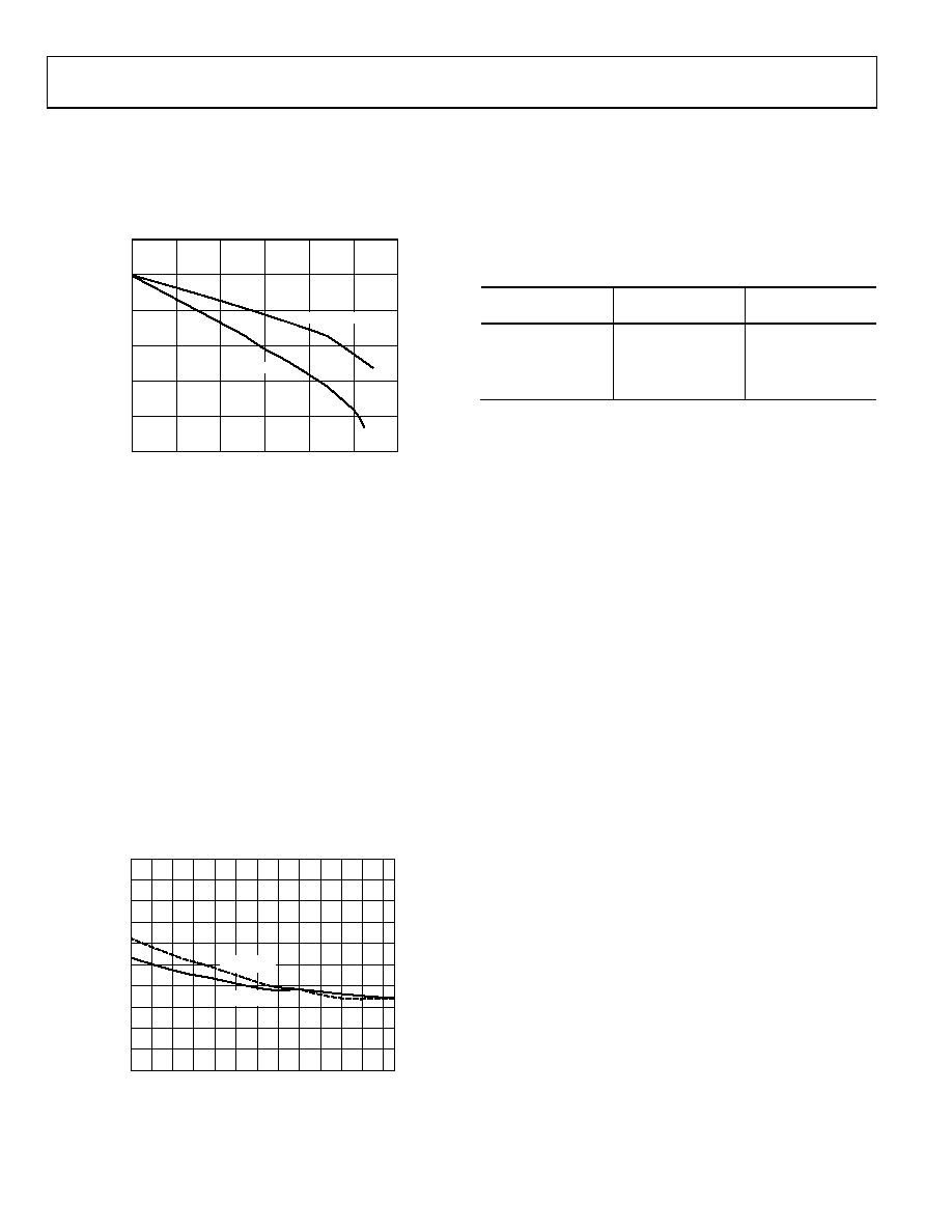
If the internal reference of the AD9236 is used to drive multiple
converters to improve gain matching, the loading of the reference
by the other converters must be considered. Figure 35 depicts
how the internal reference voltage is affected by loading. A
2 mA load is the maximum recommended load.
LOAD (mA)
E
RROR
(%
)
0.05
0
0.5
1.0
1.5
2.0
2.5
3.0
03066-0-019
0
–0.25
–0.20
–0.15
–0.10
–0.05
0.5V ERROR (%)
1.0V ERROR (%)
Figure 35. VREF Accuracy vs. Load
External Reference Operation
The use of an external reference can be necessary to enhance
the gain accuracy of the ADC or to improve thermal drift
characteristics. When multiple ADCs track one another, a
single reference (internal or external) can be necessary to
reduce gain matching errors to an acceptable level. Figure 36
shows the typical drift characteristics of the internal reference
in both 1.0 V and 0.5 V modes.
When the SENSE pin is tied to AVDD, the internal reference is
disabled, allowing the use of an external reference. An internal
reference buffer loads the external reference with an equivalent
7 kΩ load. The internal buffer still generates the positive and
negative full-scale references, REFT and REFB, for the ADC
core. The input span is always twice the value of the reference
voltage; therefore, the external reference must be limited to a
maximum of 1.0 V.
1.0
V
REF
ERRO
R
(
%
)
0
0.1
0.2
0.3
0.4
0.5
0.6
0.7
0.8
0.9
–40 –30 –20 –10
0
1020304050607080
TEMPERATURE (
C)
03066-0-011
VREF = 0.5V
VREF = 1.0V
Figure 36. Typical VREF Drift
OPERATIONAL MODE SELECTION
As discussed in the Digital Outputs section, the AD9236 can
output data in either offset binary or twos complement format.
There is also a provision for enabling or disabling the clock duty
cycle stabilizer (DCS). The MODE pin is a multilevel input that
controls the data format and DCS state. The input threshold
values and corresponding mode selections are outlined in Table 11.
Table 11. Mode Selection
MODE Voltage
Data Format
Duty Cycle
Stabilizer
AVDD
Twos Complement
Disabled
2/3 AVDD
Twos Complement
Enabled
1/3 AVDD
Offset Binary
Enabled
AGND (Default)
Offset Binary
Disabled
EVALUATION BOARD
The AD9236 evaluation board provides all of the support
circuitry required to operate the ADC in its various modes and
configurations. Complete schematics and layout plots follow
and demonstrate the proper routing and grounding techniques
that should be applied at the system level.
It is critical that signal sources with very low phase noise (< 1 ps
rms jitter) be used to realize the ultimate performance of the
converter. Proper filtering of the input signal, to remove
harmonics and lower the integrated noise at the input, is also
necessary to achieve the specified noise performance.
TSSOP Evaluation Board
Figure 37 shows the typical bench setup used to evaluate the ac
performance of the AD9236. The AD9236 can be driven single-
ended or differentially through an AD8138 driver or a
transformer. Separate power pins are provided to isolate the
DUT from the support circuitry. Each input configuration can
be selected by proper connection of various jumpers (refer to
the schematics).
The AUXCLK input should be selected in applications requiring
the lowest jitter and SNR performance (that is, IF undersampling
characterization). It allows the user to apply a clock input signal
that is 4× the target sample rate of the AD9236. A low jitter,
differential divide-by-4 counter, the MC100LVEL33D, provides
a 1× clock output that is subsequently returned back to the CLK
input via JP9. For example, a 260 MHz signal (sinusoid) is
divided down to a 65 MHz signal for clocking the ADC. Note
that R1 must be removed with the AUXCLK interface. Lower
jitter is often achieved with this interface since many RF signal
generators display improved phase noise at higher output
frequencies and the slew rate of the sinusoidal output signal is
4× that of a 1× signal of equal amplitude.
相关PDF资料 |
PDF描述 |
|---|---|
| AD9629BCPZRL7-80 | IC ADC 12BIT 80MSPS 32LFCSP |
| MS27474T20B41PC | CONN RCPT 41POS JAM NUT W/PINS |
| MS27484T12F4P | CONN PLUG 4POS STRAIGHT W/PINS |
| MS3106F16-13P | CONN PLUG 2POS STRAIGHT W/PINS |
| MS3102E22-12P | CONN RCPT 5POS BOX MNT W/PINS |
相关代理商/技术参数 |
参数描述 |
|---|---|
| AD9236BRU-80 | 制造商:Analog Devices 功能描述:IC 12BIT ADC 3V 80MSPS SMD 9236 |
| AD9236BRU-80EB | 制造商:Analog Devices 功能描述:Evaluation Board For 12-Bit, 80 MSPS, 3 V A/D Converter |
| AD9236BRURL7-80 | 制造商:Analog Devices 功能描述:ADC Single Pipelined 80Msps 12-bit Parallel 28-Pin TSSOP T/R |
| AD9236BRUZ-80 | 功能描述:IC ADC 12BIT 80MSPS 28TSSOP RoHS:是 类别:集成电路 (IC) >> 数据采集 - 模数转换器 系列:- 其它有关文件:TSA1204 View All Specifications 标准包装:1 系列:- 位数:12 采样率(每秒):20M 数据接口:并联 转换器数目:2 功率耗散(最大):155mW 电压电源:模拟和数字 工作温度:-40°C ~ 85°C 安装类型:表面贴装 封装/外壳:48-TQFP 供应商设备封装:48-TQFP(7x7) 包装:Digi-Reel® 输入数目和类型:4 个单端,单极;2 个差分,单极 产品目录页面:1156 (CN2011-ZH PDF) 其它名称:497-5435-6 |
| AD9236BRUZRL7-80 | 功能描述:IC ADC 12BIT 80MSPS 28TSSOP RoHS:是 类别:集成电路 (IC) >> 数据采集 - 模数转换器 系列:- 标准包装:1 系列:- 位数:14 采样率(每秒):83k 数据接口:串行,并联 转换器数目:1 功率耗散(最大):95mW 电压电源:双 ± 工作温度:0°C ~ 70°C 安装类型:通孔 封装/外壳:28-DIP(0.600",15.24mm) 供应商设备封装:28-PDIP 包装:管件 输入数目和类型:1 个单端,双极 |
发布紧急采购,3分钟左右您将得到回复。