- 您现在的位置:买卖IC网 > PDF目录9798 > AD9238BST-40 (Analog Devices Inc)IC ADC 12BIT DUAL 40MSPS 64-LQFP PDF资料下载
参数资料
| 型号: | AD9238BST-40 |
| 厂商: | Analog Devices Inc |
| 文件页数: | 10/48页 |
| 文件大小: | 0K |
| 描述: | IC ADC 12BIT DUAL 40MSPS 64-LQFP |
| 产品变化通告: | AD9238 Lead Discontinuation 12/Sept/2011 |
| 标准包装: | 1 |
| 位数: | 12 |
| 采样率(每秒): | 40M |
| 数据接口: | 并联 |
| 转换器数目: | 2 |
| 功率耗散(最大): | 330mW |
| 电压电源: | 单电源 |
| 工作温度: | -40°C ~ 85°C |
| 安装类型: | 表面贴装 |
| 封装/外壳: | 64-LQFP |
| 供应商设备封装: | 64-LQFP(7x7) |
| 包装: | 托盘 |
| 输入数目和类型: | 4 个单端,单极;2 个差分,单极 |
| 配用: | AD9238BCP-65EBZ-ND - BOARD EVAL WITH AD9238BCP-65 |
第1页第2页第3页第4页第5页第6页第7页第8页第9页当前第10页第11页第12页第13页第14页第15页第16页第17页第18页第19页第20页第21页第22页第23页第24页第25页第26页第27页第28页第29页第30页第31页第32页第33页第34页第35页第36页第37页第38页第39页第40页第41页第42页第43页第44页第45页第46页第47页第48页
AD9238
Rev. C | Page 18 of 48
A single channel can be powered down for moderate power
savings. The powered-down channel shuts down internal
circuits, but both the reference buffers and shared reference
remain powered on. Because the buffer and voltage reference
remain powered on, the wake-up time is reduced to several
clock cycles.
POWER DISSIPATION AND STANDBY MODE
The power dissipated by the AD9238 is proportional to its
sampling rates. The digital (DRVDD) power dissipation is
determined primarily by the strength of the digital drivers and
the load on each output bit. The digital drive current can be
calculated by
DIGITAL OUTPUTS
IDRVDD = VDRVDD × CLOAD × fCLOCK × N
The AD9238 output drivers can be configured to interface with
2.5 V or 3.3 V logic families by matching DRVDD to the digital
supply of the interfaced logic. The output drivers are sized to
provide sufficient output current to drive a wide variety of logic
families. However, large drive currents tend to cause current
glitches on the supplies that may affect converter performance.
Applications requiring the ADC to drive large capacitive loads
or large fanouts may require external buffers or latches.
where N is the number of bits changing, and CLOAD is the average
load on the digital pins that changed.
The analog circuitry is optimally biased so that each speed
grade provides excellent performance while affording reduced
power consumption. Each speed grade dissipates a baseline
power at low sample rates that increases with clock frequency.
Either channel of the AD9238 can be placed into standby mode
independently by asserting the PDWN_A or PDWN_B pins.
The data format can be selected for either offset binary or twos
complement. See the Data Format section for more information.
It is recommended that the input clock(s) and analog input(s)
remain static during either independent or total standby, which
results in a typical power consumption of 1 mW for the ADC.
Note that if DCS is enabled, it is mandatory to disable the clock
of an independently powered-down channel. Otherwise,
significant distortion results on the active channel. If the clock
inputs remain active while in total standby mode, typical power
dissipation of 12 mW results.
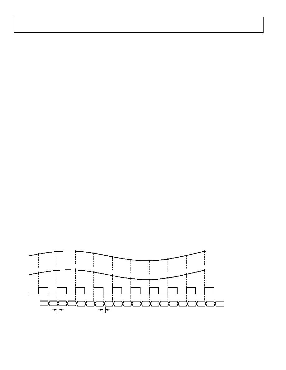
TIMING
The AD9238 provides latched data outputs with a pipeline delay
of seven clock cycles. Data outputs are available one propa-
gation delay (tPD) after the rising edge of the clock signal. Refer
to Figure 2 for a detailed timing diagram.
The internal duty cycle stabilizer can be enabled on the AD9238
using the DCS pin. This provides a stable 50% duty cycle to
internal circuits.
The minimum standby power is achieved when both channels
are placed into full power-down mode (PDWN_A = PDWN_B =
HI). Under this condition, the internal references are powered
down. When either or both of the channel paths are enabled after a
power-down, the wake-up time is directly related to the recharging
of the REFT and REFB decoupling capacitors and to the duration
of the power-down. Typically, it takes approximately 5 ms to
restore full operation with fully discharged 0.1 μF and 10 μF
decoupling capacitors on REFT and REFB.
The length of the output data lines and loads placed on them
should be minimized to reduce transients within the AD9238.
These transients can detract from the converter’s dynamic
performance. The lowest typical conversion rate of the AD9238
is 1 MSPS. At clock rates below 1 MSPS, dynamic performance
may degrade.
B–8
A–7
B–7
A–6
B–6
A–5
B–5
A–4
B–4
A–3
B–3
A–2
B–2
A–1
B–1
A0
B0
A1
A–1
A0
A1
A2
A3
A4
A5
A6
A7
A8
B–1
B0
B1
B2
B3
B4
B5
B6
B7
B8
ANALOG INPUT
ADC A
ANALOG INPUT
ADC B
CLK_A = CLK_B =
MUX_SELECT
D0_A TO
D11_A
tPD
02640-066
Figure 34. Multiplexed Data Format Using the Channel A Output and the Same Clock Tied to CLK_A, CLK_B, and MUX_SELECT
相关PDF资料 |
PDF描述 |
|---|---|
| VI-2TF-MX-F3 | CONVERTER MOD DC/DC 72V 75W |
| MAX3223EEAP | IC TXRX RS232 250KBPS SD 20-SSOP |
| VI-23F-IU-F3 | CONVERTER MOD DC/DC 72V 200W |
| VI-2TF-MX-F1 | CONVERTER MOD DC/DC 72V 75W |
| MAX3386EEUP+T | IC TXRX RS232 250KBPS 20-TSSOP |
相关代理商/技术参数 |
参数描述 |
|---|---|
| AD9238BST-40EBZ | 制造商:Analog Devices 功能描述:Evaluation Board For AD9238 Dual A/D Converter ,12-Bit, 20 MSPS/40 MSPS/65 MSPS 制造商:Analog Devices 功能描述:EVAL BD FOR AD9238 DUAL A/D CNVRTR ,12-BIT, 20 MSPS/40 MSPS/ - Bulk |
| AD9238BST-40PCB | 制造商:Analog Devices 功能描述:Evaluation Board For AD9238 Dual A/D Converter ,12-Bit, 20 MSPS/40 MSPS/65 MSPS 制造商:Analog Devices 功能描述:EVAL BD FOR AD9238 DUAL A/D CNVRTR ,12-BIT, 20 MSPS/40 MSPS/ - Bulk |
| AD9238BST-40PCBZ | 制造商:Analog Devices 功能描述:DUAL 12 BIT 3V CMOS 20/40/65 MSPS ADC - Bulk |
| AD9238BST-65 | 功能描述:IC ADC 12BIT DUAL 65MSPS 64-LQFP RoHS:否 类别:集成电路 (IC) >> 数据采集 - 模数转换器 系列:- 产品培训模块:Lead (SnPb) Finish for COTS Obsolescence Mitigation Program 标准包装:2,500 系列:- 位数:12 采样率(每秒):3M 数据接口:- 转换器数目:- 功率耗散(最大):- 电压电源:- 工作温度:- 安装类型:表面贴装 封装/外壳:SOT-23-6 供应商设备封装:SOT-23-6 包装:带卷 (TR) 输入数目和类型:- |
| AD9238BST-65PCB | 制造商:Analog Devices 功能描述:Evaluation Board For AD9238 Dual A/D Converter ,12-Bit, 20 MSPS/40 MSPS/65 MSPS 制造商:Rochester Electronics LLC 功能描述:DUAL 12 BIT 3V CMOS 20/40/65 MSPS ADC - Bulk |
发布紧急采购,3分钟左右您将得到回复。