- 您现在的位置:买卖IC网 > PDF目录10658 > AD9244BSTZ-40 (Analog Devices Inc)IC ADC 14BIT 40MSPS 48-LQFP PDF资料下载
参数资料
| 型号: | AD9244BSTZ-40 |
| 厂商: | Analog Devices Inc |
| 文件页数: | 14/36页 |
| 文件大小: | 0K |
| 描述: | IC ADC 14BIT 40MSPS 48-LQFP |
| 标准包装: | 1 |
| 位数: | 14 |
| 采样率(每秒): | 40M |
| 数据接口: | 并联 |
| 转换器数目: | 1 |
| 功率耗散(最大): | 300mW |
| 电压电源: | 模拟和数字 |
| 工作温度: | -40°C ~ 85°C |
| 安装类型: | 表面贴装 |
| 封装/外壳: | 48-LQFP |
| 供应商设备封装: | 48-LQFP(7x7) |
| 包装: | 托盘 |
| 输入数目和类型: | 2 个单端,单极;1 个差分,单极 |
第1页第2页第3页第4页第5页第6页第7页第8页第9页第10页第11页第12页第13页当前第14页第15页第16页第17页第18页第19页第20页第21页第22页第23页第24页第25页第26页第27页第28页第29页第30页第31页第32页第33页第34页第35页第36页
AD9244
Rev. C | Page 21 of 36
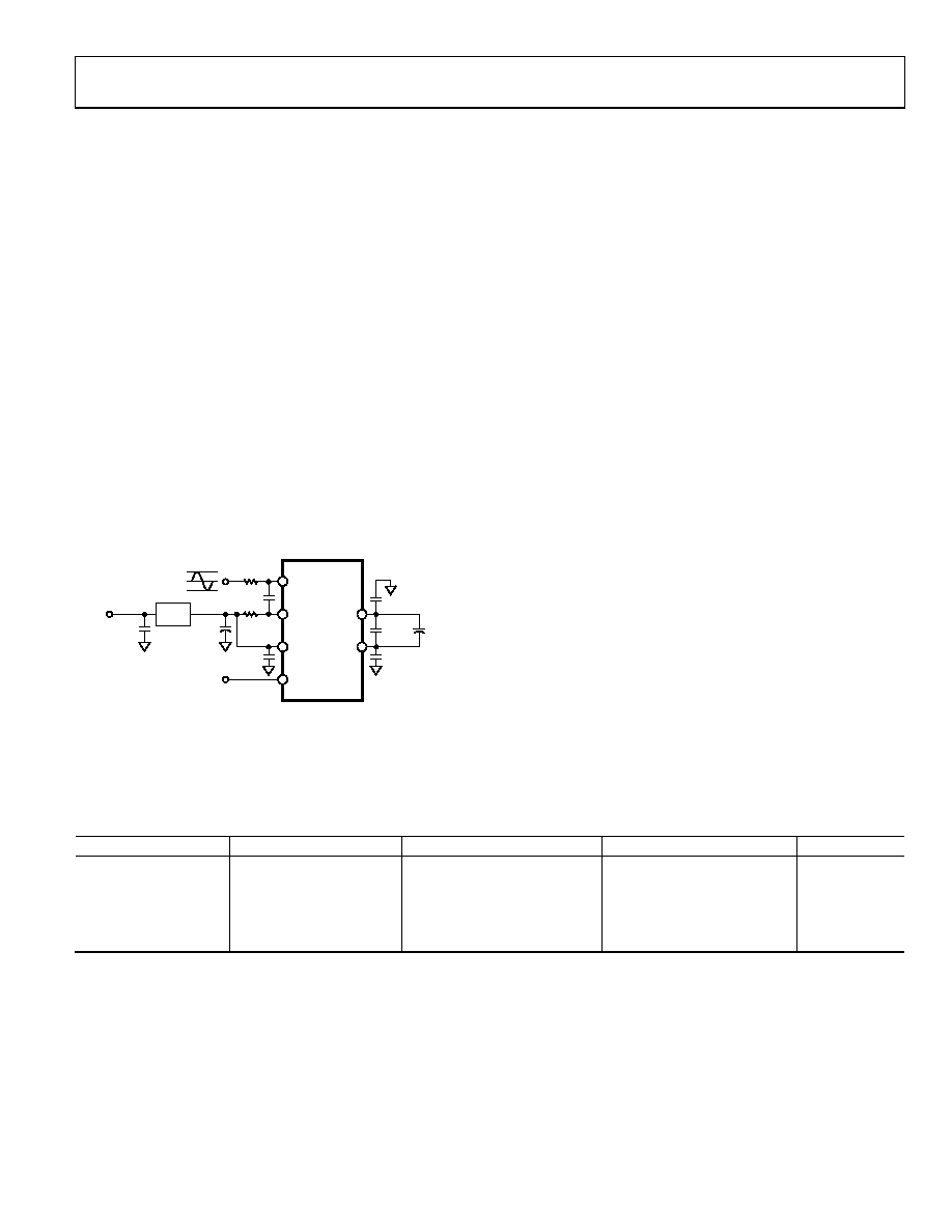
Using an External Reference
To use an external reference, the internal reference must be dis-
abled by connecting the SENSE pin to AVDD. The AD9244
contains an internal reference buffer, A2 (see Figure 48), that
simplifies the drive requirements of an external reference. The
external reference must be able to drive a 5 kΩ (±20%) load.
The bandwidth of the reference is deliberately left small to
minimize the reference noise contribution. As a result, it is not
possible to drive VREF externally with high frequencies.
Figure 51 shows an example of an external reference driving
both VIN– and VREF. In this case, both the common-mode
voltage and input span are directly dependent on the value of
VREF. Both the input span and the center of the input span are
equal to the external VREF. Thus, the valid input range extends
from (VREF + VREF/2) to (VREF VREF/2). For example, if
the Precision Reference Part REF191, a 2.048 V external refer-
ence, is used, the input span is 2.048 V. In this case, 1 LSB of the
AD9244 corresponds to 0.125 mV.
It is essential that a minimum of a 10 μF capacitor, in parallel
with a 0.1 μF low inductance ceramic capacitor, decouple the
reference output to AGND.
5V
AVDD
REFT
REFB
VREF
SENSE
AD9244
VIN+
VIN–
33
Ω
20pF
0.1
μF
0.1
μF
0.1
μF
0.1
μF
0.1
μF
10
μF
10
μF
33
Ω
+
VREF + VREF/2
VREF – VREF/2
VREF
02
40
4-
05
1
Figure 51. Using an External Reference
Digital Outputs
Table 10 details the relationship among the ADC input, OTR,
and digital output format.
Data Format Select (DFS)
The AD9244 can be programmed for straight binary or twos
complement data on the digital outputs. Connect the DFS pin to
AGND for straight binary and to AVDD for twos complement.
Digital Output Driver Considerations
The AD9244 output drivers can be configured to interface with
5 V or 3.3 V logic families by setting DRVDD to 5 V or 3.3 V,
respectively. The output drivers are sized to provide sufficient
output current to drive a wide variety of logic families.
However, large drive currents tend to cause glitches on the
supplies and can affect converter performance. Applications
requiring the ADC to drive large capacitive loads or large
fanouts can require external buffers or latches.
DIGITAL INPUTS AND OUTPUTS
Table 10. Output Data Format
Input (V)
Condition (V)
Binary Output Mode
Twos Complement Mode
OTR
VIN+ – VIN
< –VREF/2 0.5 LSB
00 0000 0000 0000
10 0000 0000 0000
1
VIN+ – VIN
= VREF/2
00 0000 0000 0000
10 0000 0000 0000
0
VIN+ – VIN
= 0
10 0000 0000 0000
00 0000 0000 0000
0
VIN+ – VIN
= +VREF/2 1.0 LSB
11 1111 1111 1111
01 1111 1111 1111
0
VIN+ – VIN
> +VREF/2 0.5 LSB
11 1111 1111 1111
01 1111 1111 1111
1
相关PDF资料 |
PDF描述 |
|---|---|
| VI-J7V-MY-F4 | CONVERTER MOD DC/DC 5.8V 50W |
| MAX981ESA+ | IC COMPARATOR OD 8-SOIC |
| VI-J7V-MY-F3 | CONVERTER MOD DC/DC 5.8V 50W |
| MAX972EPA+ | IC COMPARATOR OD 8-DIP |
| MAX981EPA+ | IC COMPARATOR OD 8-DIP |
相关代理商/技术参数 |
参数描述 |
|---|---|
| AD9244BSTZ-401 | 制造商:AD 制造商全称:Analog Devices 功能描述:14-Bit, 40 MSPS/65 MSPS A/D Converter |
| AD9244BSTZ-65 | 功能描述:IC ADC 14BIT 65MSPS 48-LQFP RoHS:是 类别:集成电路 (IC) >> 数据采集 - 模数转换器 系列:- 标准包装:1 系列:microPOWER™ 位数:8 采样率(每秒):1M 数据接口:串行,SPI? 转换器数目:1 功率耗散(最大):- 电压电源:模拟和数字 工作温度:-40°C ~ 125°C 安装类型:表面贴装 封装/外壳:24-VFQFN 裸露焊盘 供应商设备封装:24-VQFN 裸露焊盘(4x4) 包装:Digi-Reel® 输入数目和类型:8 个单端,单极 产品目录页面:892 (CN2011-ZH PDF) 其它名称:296-25851-6 |
| AD9244BSTZ-65 | 制造商:Analog Devices 功能描述:IC 14BIT ADC SMD 9244 LQFP48 制造商:Analog Devices 功能描述:IC, 14BIT ADC, SMD, 9244, LQFP48 |
| AD9244BSTZ-651 | 制造商:AD 制造商全称:Analog Devices 功能描述:14-Bit, 40 MSPS/65 MSPS A/D Converter |
| AD9244BSTZRL-40 | 功能描述:IC ADC 14BIT SGL 40MSPS 48LQFP RoHS:是 类别:集成电路 (IC) >> 数据采集 - 模数转换器 系列:- 标准包装:1 系列:- 位数:14 采样率(每秒):83k 数据接口:串行,并联 转换器数目:1 功率耗散(最大):95mW 电压电源:双 ± 工作温度:0°C ~ 70°C 安装类型:通孔 封装/外壳:28-DIP(0.600",15.24mm) 供应商设备封装:28-PDIP 包装:管件 输入数目和类型:1 个单端,双极 |
发布紧急采购,3分钟左右您将得到回复。