- 您现在的位置:买卖IC网 > PDF目录10113 > AD9245BCPZRL7-65 (Analog Devices Inc)IC ADC 14BIT SGL 65MSPS 32LFCSP PDF资料下载
参数资料
| 型号: | AD9245BCPZRL7-65 |
| 厂商: | Analog Devices Inc |
| 文件页数: | 11/32页 |
| 文件大小: | 0K |
| 描述: | IC ADC 14BIT SGL 65MSPS 32LFCSP |
| 标准包装: | 1,500 |
| 位数: | 14 |
| 采样率(每秒): | 65M |
| 数据接口: | 并联 |
| 转换器数目: | 3 |
| 功率耗散(最大): | 300mW |
| 电压电源: | 单电源 |
| 工作温度: | -40°C ~ 85°C |
| 安装类型: | 表面贴装 |
| 封装/外壳: | 32-VFQFN 裸露焊盘,CSP |
| 供应商设备封装: | 32-LFCSP-VQ(5x5) |
| 包装: | 带卷 (TR) |
| 输入数目和类型: | 2 个单端,单极;1 个差分,单极 |
第1页第2页第3页第4页第5页第6页第7页第8页第9页第10页当前第11页第12页第13页第14页第15页第16页第17页第18页第19页第20页第21页第22页第23页第24页第25页第26页第27页第28页第29页第30页第31页第32页
Data Sheet
AD9245
Rev. E | Page 19 of 32
The SHA can be driven from a source that keeps the signal
peaks within the allowable range for the selected reference
voltage. The minimum and maximum common-mode input
levels are defined as
2
VREF
VCMMIN =
(
)
2
VREF
AVDD
VCMMAX
+
=
The minimum common-mode input level allows the AD9245 to
accommodate ground referenced inputs.
Although optimum performance is achieved with a differential
input, a single-ended source can be applied to VIN+ or VIN–.
In this configuration, one input accepts the signal, while the
opposite input is set to midscale by connecting it to an
appropriate reference. For example, a 2 V p-p signal can be
applied to VIN+ while a 1 V reference is applied to VIN–. The
AD9245 then accepts an input signal varying between 2 V and
0 V. In the single-ended configuration, distortion performance
can degrade significantly as compared to the differential case.
However, the effect is less noticeable at lower input frequencies.
Differential Input Configurations
As previously detailed, optimum performance is achieved while
driving the AD9245 in a differential input configuration. For
baseband applications, the AD8351 differential driver provides
excellent performance and a flexible interface to the ADC. The
output common-mode voltage of the AD8351 is easily set to
AVDD/2, and the driver can be configured in a Sallen-Key filter
topology to provide band limiting of the input signal.
03583
-013
AD9245
VIN+
VIN–
AGND
AVDD
2V p-p
33
20pF
AD8351
1k
0.1F
1.2k
25
0.1mF
25
50
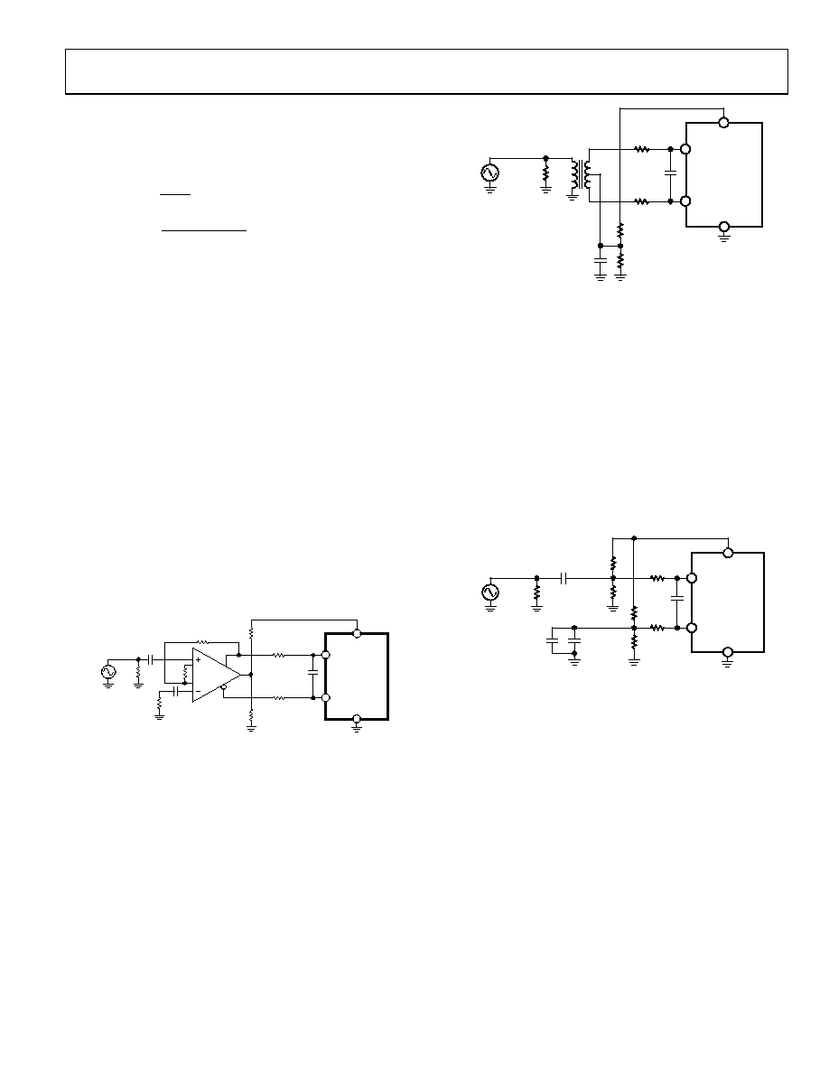
Figure 40. Differential Input Configuration Using the AD8351
At input frequencies in the second Nyquist zone and above, the
performance of most amplifiers is not adequate to achieve the
true performance of the AD9245. This is especially true in IF
undersampling applications where frequencies in the 70 MHz to
100 MHz range are being sampled. For these applications,
differential transformer coupling is the recommended input
configuration. The value of the shunt capacitor is dependent on
the input frequency and source impedance and should be
reduced or removed. An example is shown in Figure 41.
03583-
014
AD9245
VIN+
VIN–
AVDD
AGND
33
33
20pF
49.9
1k
1k
0.1
F
2V p-p
Figure 41. Differential Transformer-Coupled Configuration
The signal characteristics must be considered when selecting
a transformer. Most RF transformers saturate at frequencies
below a few MHz, and excessive signal power can also cause
core saturation, which leads to distortion.
Single-Ended Input Configuration
A single-ended input can provide adequate performance in
cost-sensitive applications. In this configuration, there is a
degradation in SFDR and distortion performance due to the
large input common-mode swing (see Figure 13). However, if
the source impedances on each input are matched, there should
be little effect on SNR performance. Figure 42 details a typical
single-ended input configuration.
03583-
015
AD9245
VIN+
VIN–
AVDD
AGND
2V p-p
33
33
20pF
49.9
1k
1k
0.33
F
10
F
0.1
F
1k
1k
+
Figure 42. Single-Ended Input Configuration
CLOCK INPUT CONSIDERATIONS
Typical high speed ADCs use both clock edges to generate a
variety of internal timing signals, and as a result can be sensitive
to clock duty cycle. Commonly a 5% tolerance is required on the
clock duty cycle to maintain dynamic performance characteristics.
The AD9245-80 and AD9245-65 contain a clock duty cycle
stabilizer (DCS) that retimes the nonsampling edge, providing an
internal clock signal with a nominal 50% duty cycle. This allows a
wide range of clock input duty cycles without affecting the
performance of the AD9245. As shown in Figure 21, noise and
distortion performance is nearly flat for a 30% to 70% duty cycle
with the DCS on.
The duty cycle stabilizer uses a delay-locked loop (DLL) to
create the nonsampling edge. As a result, any changes to the
sampling frequency require approximately 100 clock cycles to
allow the DLL to acquire and lock to the new rate.
相关PDF资料 |
PDF描述 |
|---|---|
| VI-2NX-MX-F4 | CONVERTER MOD DC/DC 5.2V 75W |
| VE-23P-IW-F3 | CONVERTER MOD DC/DC 13.8V 100W |
| LTC2234IUK#TR | IC ADC 10BIT 135MSPS SAMPL 48QFN |
| LTC2864CDD-1#PBF | IC TRANSCEIVER RS485 10-DFN |
| VE-23P-IW-F2 | CONVERTER MOD DC/DC 13.8V 100W |
相关代理商/技术参数 |
参数描述 |
|---|---|
| AD9245BCPZRL7-652 | 制造商:AD 制造商全称:Analog Devices 功能描述:14-Bit, 20 MSPS/40 MSPS/65 MSPS/80 MSPS, 3 V A/D Converter |
| AD9245BCPZRL7-80 | 功能描述:IC ADC 14BIT SGL 80MSPS 32LFCSP RoHS:是 类别:集成电路 (IC) >> 数据采集 - 模数转换器 系列:- 标准包装:1 系列:- 位数:14 采样率(每秒):83k 数据接口:串行,并联 转换器数目:1 功率耗散(最大):95mW 电压电源:双 ± 工作温度:0°C ~ 70°C 安装类型:通孔 封装/外壳:28-DIP(0.600",15.24mm) 供应商设备封装:28-PDIP 包装:管件 输入数目和类型:1 个单端,双极 |
| AD9245BCPZRL7-802 | 制造商:AD 制造商全称:Analog Devices 功能描述:14-Bit, 20 MSPS/40 MSPS/65 MSPS/80 MSPS, 3 V A/D Converter |
| AD9245BPCZ-80 | 制造商:Analog Devices 功能描述:14BIT 80MSPS - Bulk 制造商:Analog Devices 功能描述:Analog Devices AD9245BPCZ-80 Data Conversions |
| AD9245XCPZ-20 | 制造商:Analog Devices 功能描述:40 MSPS DUAL A/D CONVERTER - Bulk |
发布紧急采购,3分钟左右您将得到回复。