- 您现在的位置:买卖IC网 > PDF目录10527 > AD9248BCPZ-20 (Analog Devices Inc)IC ADC 14BIT DUAL 20MSPS 64LFCSP PDF资料下载
参数资料
| 型号: | AD9248BCPZ-20 |
| 厂商: | Analog Devices Inc |
| 文件页数: | 10/48页 |
| 文件大小: | 0K |
| 描述: | IC ADC 14BIT DUAL 20MSPS 64LFCSP |
| 标准包装: | 1 |
| 位数: | 14 |
| 采样率(每秒): | 20M |
| 数据接口: | 并联 |
| 转换器数目: | 2 |
| 功率耗散(最大): | 180mW |
| 电压电源: | 单电源 |
| 工作温度: | -40°C ~ 85°C |
| 安装类型: | 表面贴装 |
| 封装/外壳: | 64-VFQFN 裸露焊盘,CSP |
| 供应商设备封装: | 64-LFCSP-VQ(9x9) |
| 包装: | 托盘 |
| 输入数目和类型: | 4 个单端,单极;2 个差分,单极 |
第1页第2页第3页第4页第5页第6页第7页第8页第9页当前第10页第11页第12页第13页第14页第15页第16页第17页第18页第19页第20页第21页第22页第23页第24页第25页第26页第27页第28页第29页第30页第31页第32页第33页第34页第35页第36页第37页第38页第39页第40页第41页第42页第43页第44页第45页第46页第47页第48页
AD9248
Rev. B | Page 18 of 48
The minimum common-mode input level allows the AD9248 to
accommodate ground-referenced inputs. Although optimum
performance is achieved with a differential input, a single-ended
source may be driven into VIN+ or VIN. In this configuration,
one input accepts the signal, while the opposite input should be
set to midscale by connecting it to an appropriate reference. For
example, a 2 V p-p signal may be applied to VIN+, while a 1 V
reference is applied to VIN. The AD9248 then accepts an
input signal varying between 2 V and 0 V. In the single-ended
configuration, distortion performance may degrade significantly
as compared to the differential case. However, the effect is less
noticeable at lower input frequencies and in the lower speed grade
models (AD9248-40 and AD9248-20).
Differential Input Configurations
As previously detailed, optimum performance is achieved while
driving the AD9248 in a differential input configuration. For
baseband applications, the AD8138 differential driver provides
excellent performance and a flexible interface to the ADC. The
output common-mode voltage of the AD8138 is easily set to
AVDD/2, and the driver can be configured in a Sallen-Key filter
topology to provide band limiting of the input signal.
At input frequencies in the second Nyquist zone and above, the
performance of most amplifiers is not adequate to achieve the
true performance of the AD9248. This is especially true in IF
under-sampling applications where frequencies in the 70 MHz
to 200 MHz range are being sampled. For these applications,
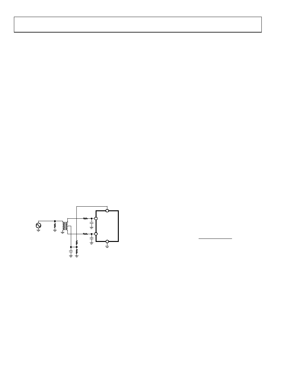
differential transformer coupling is the recommended input
configuration, as shown in Figure 33.
AD9248
VINA
VINB
AVDD
AGND
2V p-p
50
Ω
50
Ω
10pF
49.9
Ω
1k
Ω
1k
Ω
0.1
μF
04446-032
Figure 33. Differential Transformer Coupling
The signal characteristics must be considered when selecting a
transformer. Most RF transformers saturate at frequencies
below a few MHz, and excessive signal power can also cause
core saturation, which leads to distortion.
Single-Ended Input Configuration
A single-ended input may provide adequate performance in
cost-sensitive applications. In this configuration, there is a
degradation in SFDR and distortion performance due to the
large input common-mode swing. However, if the source
impedances on each input are matched, there should be little
effect on SNR performance.
CLOCK INPUT AND CONSIDERATIONS
Typical high speed ADCs use both clock edges to generate a
variety of internal timing signals and, as a result, may be sensitive
to the clock duty cycle. Commonly, a 5% tolerance is required
on the clock duty cycle to maintain dynamic performance
characteristics.
The AD9248 provides separate clock inputs for each channel. The
optimum performance is achieved with the clocks operated at the
same frequency and phase. Clocking the channels asynchronously
may degrade performance significantly. In some applications, it
is desirable to skew the clock timing of adjacent channels. The
AD9248’s separate clock inputs allow for clock timing skew
(typically ±1 ns) between the channels without significant
performance degradation.
The AD9248-65 contains two clock duty cycle stabilizers, one
for each converter, that retime the nonsampling edge, providing
an internal clock with a nominal 50% duty cycle. When proper
track-and-hold times for the converter are required to maintain
high performance, maintaining a 50% duty cycle clock is
particularly important in high speed applications. It may be
difficult to maintain a tightly controlled duty cycle on the input
clock on the PCB (see Figure 24). DCS can be enabled by tying
the DCS pin high.
The duty cycle stabilizer uses a delay-locked loop to create the
nonsampling edge. As a result, any changes to the sampling
frequency require approximately 2 μs to 3 μs to allow the DLL
to acquire and settle to the new rate.
High speed, high resolution ADCs are sensitive to the quality of
the clock input. The degradation in SNR at a given full-scale
input frequency (fINPUT) due only to aperture jitter (tJ) can be
calculated as
()
×
=
j
INPUT
t
f
π
SNR
2
1
log
20
In the equation, the rms aperture jitter, tJ , represents the root-
sum square of all jitter sources, which includes the clock input,
analog input signal, and ADC aperture jitter specification.
Under-sampling applications are particularly sensitive to jitter.
For optimal performance, especially in cases where aperture
jitter may affect the dynamic range of the AD9248, it is important
to minimize input clock jitter. The clock input circuitry should
use stable references; for example, use analog power and ground
planes to generate the valid high and low digital levels for the
AD9248 clock input. Power supplies for clock drivers should be
separated from the ADC output driver supplies to avoid modulating
the clock signal with digital noise. Low jitter, crystal-controlled
oscillators make the best clock sources. If the clock is generated from
another type of source (by gating, dividing, or other methods), it
should be retimed by the original clock at the last step.
相关PDF资料 |
PDF描述 |
|---|---|
| MS3102E24-12P | CONN RCPT 5POS BOX MNT W/PINS |
| NCV7356D1G | IC TXRX CAN SGL WIRE 8-SOIC |
| LTC2392CUK-16#PBF | IC ADC 16BIT SER/PAR 500K 48QFN |
| PT01E-10-6P | CONN RCPT 6 POS CBL MNT W/PINS |
| AD9634BCPZ-170 | IC ADC 12BIT 170MSPS 32-LFCSP |
相关代理商/技术参数 |
参数描述 |
|---|---|
| AD9248BCPZ-40 | 功能描述:IC ADC 14BIT DUAL 40MSPS 64LFCSP RoHS:是 类别:集成电路 (IC) >> 数据采集 - 模数转换器 系列:- 其它有关文件:TSA1204 View All Specifications 标准包装:1 系列:- 位数:12 采样率(每秒):20M 数据接口:并联 转换器数目:2 功率耗散(最大):155mW 电压电源:模拟和数字 工作温度:-40°C ~ 85°C 安装类型:表面贴装 封装/外壳:48-TQFP 供应商设备封装:48-TQFP(7x7) 包装:Digi-Reel® 输入数目和类型:4 个单端,单极;2 个差分,单极 产品目录页面:1156 (CN2011-ZH PDF) 其它名称:497-5435-6 |
| AD9248BCPZ-65 | 功能描述:IC ADC 14BIT DUAL 65MSPS 64LFCSP RoHS:是 类别:集成电路 (IC) >> 数据采集 - 模数转换器 系列:- 其它有关文件:TSA1204 View All Specifications 标准包装:1 系列:- 位数:12 采样率(每秒):20M 数据接口:并联 转换器数目:2 功率耗散(最大):155mW 电压电源:模拟和数字 工作温度:-40°C ~ 85°C 安装类型:表面贴装 封装/外壳:48-TQFP 供应商设备封装:48-TQFP(7x7) 包装:Digi-Reel® 输入数目和类型:4 个单端,单极;2 个差分,单极 产品目录页面:1156 (CN2011-ZH PDF) 其它名称:497-5435-6 |
| AD9248BCPZRL-20 | 功能描述:IC ADC 14BIT DUAL 20MSPS 64LFCSP RoHS:是 类别:集成电路 (IC) >> 数据采集 - 模数转换器 系列:- 标准包装:1 系列:- 位数:14 采样率(每秒):83k 数据接口:串行,并联 转换器数目:1 功率耗散(最大):95mW 电压电源:双 ± 工作温度:0°C ~ 70°C 安装类型:通孔 封装/外壳:28-DIP(0.600",15.24mm) 供应商设备封装:28-PDIP 包装:管件 输入数目和类型:1 个单端,双极 |
| AD9248BCPZRL-40 | 功能描述:IC ADC 14BIT DUAL 40MSPS 64LFCSP RoHS:是 类别:集成电路 (IC) >> 数据采集 - 模数转换器 系列:- 标准包装:1 系列:- 位数:14 采样率(每秒):83k 数据接口:串行,并联 转换器数目:1 功率耗散(最大):95mW 电压电源:双 ± 工作温度:0°C ~ 70°C 安装类型:通孔 封装/外壳:28-DIP(0.600",15.24mm) 供应商设备封装:28-PDIP 包装:管件 输入数目和类型:1 个单端,双极 |
| AD9248BCPZRL-65 | 功能描述:IC ADC 14BIT DUAL 65MSPS 64LFCSP RoHS:是 类别:集成电路 (IC) >> 数据采集 - 模数转换器 系列:- 标准包装:1 系列:- 位数:14 采样率(每秒):83k 数据接口:串行,并联 转换器数目:1 功率耗散(最大):95mW 电压电源:双 ± 工作温度:0°C ~ 70°C 安装类型:通孔 封装/外壳:28-DIP(0.600",15.24mm) 供应商设备封装:28-PDIP 包装:管件 输入数目和类型:1 个单端,双极 |
发布紧急采购,3分钟左右您将得到回复。