- 您现在的位置:买卖IC网 > PDF目录9471 > AD9273BSVZ-25 (Analog Devices Inc)IC ADC OCT 12BIT 25MSPS 100-TQFP PDF资料下载
参数资料
| 型号: | AD9273BSVZ-25 |
| 厂商: | Analog Devices Inc |
| 文件页数: | 16/48页 |
| 文件大小: | 0K |
| 描述: | IC ADC OCT 12BIT 25MSPS 100-TQFP |
| 标准包装: | 1 |
| 类型: | AAF,ADC,交叉点开关,LNA,VGA |
| 分辨率(位): | 12 b |
| 采样率(每秒): | 25M |
| 数据接口: | 串行,SPI? |
| 电压电源: | 模拟和数字 |
| 电源电压: | 1.8V,3V |
| 工作温度: | -40°C ~ 85°C |
| 安装类型: | 表面贴装 |
| 封装/外壳: | 100-TQFP 裸露焊盘 |
| 供应商设备封装: | 100-TQFP-EP(14x14) |
| 包装: | 托盘 |
第1页第2页第3页第4页第5页第6页第7页第8页第9页第10页第11页第12页第13页第14页第15页当前第16页第17页第18页第19页第20页第21页第22页第23页第24页第25页第26页第27页第28页第29页第30页第31页第32页第33页第34页第35页第36页第37页第38页第39页第40页第41页第42页第43页第44页第45页第46页第47页第48页
AD9273
Rev. B | Page 23 of 48
Active Impedance Matching
The LNA consists of a single-ended voltage gain amplifier with
differential outputs and the negative output available externally.
For example, with a fixed gain of 8× (17.9 dB), an active input
termination is synthesized by connecting a feedback resistor
between the negative output pin, LO-x, and the positive input pin,
LI-x. This well-known technique is used for interfacing multiple
probe impedances to a single system. The input resistance is
shown in Equation 1.
)
2
1
(
A
R
FB
IN
+
=
(1)
where A/2 is the single-ended gain or the gain from the LI-x
inputs to the LO-x outputs, and RFB is the resulting impedance
Because the amplifier has a gain of 8× from its input to its
differential output, it is important to note that the gain A/2 is
the gain from Pin LI-x to Pin LO-x, and it is 6 dB less than the
gain of the amplifier, or 12.1 dB (4×). The input resistance is
reduced by an internal bias resistor of 15 kΩ in parallel with the
source resistance connected to Pin LI-x while Pin LG-x is ac
grounded. Equation 2 can be used to calculate the needed RFB
for a desired RIN, even for higher values of RIN.
Ω
+
=
k
15
||
)
3
1
(
FB
IN
R
(2)
For example, to set RIN to 200 Ω, the value of RFB must be
1000 Ω. If the simplified equation (Equation 2) is used to
calculate RIN, the value is 188 Ω, resulting in a gain error less
than 0.6 dB. Some factors, such as the presence of a dynamic
source resistance, might influence the absolute gain accuracy
more significantly. At higher frequencies, the input capacitance
of the LNA needs to be considered. The user must determine
the level of matching accuracy and adjust RFB accordingly.
The bandwidth (BW) of the LNA is greater than 100 MHz.
Ultimately, the BW of the LNA limits the accuracy of the
synthesized RIN. For RIN = RS up to about 200 Ω, the best match
is between 100 kHz and 10 MHz, where the lower frequency
limit is determined by the size of the ac-coupling capacitors,
and the upper limit is determined by the LNA BW. Furthermore,
the input capacitance and RS limit the BW at higher frequencies.
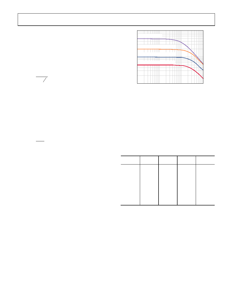
10
100
1k
100k
1M
10M
100M
INP
UT
RE
S
IS
T
A
NCE
(
)
FREQUENCY (Hz)
RS = 50, RFB = 200, CSH = 70pF
RS = 100, RFB = 400, CSH = 20pF
RS = 200, RFB = 800
RS = 500, RFB = 2k
07
03
0-
1
88
Figure 40. RIN vs. Frequency for Various Values of RFB
(Effects of RS and CSH Are Also Shown)
Note that at the lowest value (50 Ω), RIN peaks at frequencies
greater than 10 MHz. This is due to the BW roll-off of the LNA,
as mentioned previously.
However, as can be seen for larger RIN values, parasitic capacitance
starts rolling off the signal BW before the LNA can produce
peaking. CSH further degrades the match; therefore, CSH should
lists the recommended values for RFB and CSH in terms of RIN.
CFB is needed in series with RFB because the dc levels at Pin LO-x
and Pin LI-x are unequal.
Table 7. Active Termination External Component Values
LNA Gain
(dB)
RIN (Ω)
RFB (Ω)
Minimum
CSH (pF)
BW (MHz)
15.6
50
200
90
57
17.9
50
250
70
69
21.3
50
350
50
88
15.6
100
400
30
57
17.9
100
500
20
69
21.3
100
700
10
88
15.6
200
800
N/A
72
17.9
200
1000
N/A
72
21.3
200
1400
N/A
72
相关PDF资料 |
PDF描述 |
|---|---|
| LTC6905HS5-96#TRPBF | IC OSC SILICON 96MHZ TSOT23-5 |
| LTC6905HS5-80#TRPBF | IC OSC SILICON 80MHZ TSOT23-5 |
| AD7874BNZ | IC DAS 12BIT 4CH 5V 28-DIP |
| V28A15M200BL | CONVERTER MOD DC/DC 15V 200W |
| LTC6905HS5-100#TRPBF | IC OSC SILICON 100MHZ TSOT23-5 |
相关代理商/技术参数 |
参数描述 |
|---|---|
| AD9273BSVZ-40 | 功能描述:IC ADC OCT 12BIT 40MSPS 100-TQFP RoHS:是 类别:集成电路 (IC) >> 数据采集 - ADCs/DAC - 专用型 系列:- 产品培训模块:Lead (SnPb) Finish for COTS Obsolescence Mitigation Program 标准包装:50 系列:- 类型:数据采集系统(DAS) 分辨率(位):16 b 采样率(每秒):21.94k 数据接口:MICROWIRE?,QSPI?,串行,SPI? 电压电源:模拟和数字 电源电压:1.8 V ~ 3.6 V 工作温度:-40°C ~ 85°C 安装类型:表面贴装 封装/外壳:40-WFQFN 裸露焊盘 供应商设备封装:40-TQFN-EP(6x6) 包装:托盘 |
| AD9273BSVZ-50 | 功能描述:IC ADC ASD OCTAL 50MSPS 100-TQFP RoHS:是 类别:集成电路 (IC) >> 数据采集 - ADCs/DAC - 专用型 系列:- 产品培训模块:Lead (SnPb) Finish for COTS Obsolescence Mitigation Program 标准包装:50 系列:- 类型:数据采集系统(DAS) 分辨率(位):16 b 采样率(每秒):21.94k 数据接口:MICROWIRE?,QSPI?,串行,SPI? 电压电源:模拟和数字 电源电压:1.8 V ~ 3.6 V 工作温度:-40°C ~ 85°C 安装类型:表面贴装 封装/外壳:40-WFQFN 裸露焊盘 供应商设备封装:40-TQFN-EP(6x6) 包装:托盘 |
| AD9273BSVZRL-25 | 功能描述:模数转换器 - ADC 12Bit 25 MSPS Octal ADC RoHS:否 制造商:Analog Devices 通道数量: 结构: 转换速率: 分辨率: 输入类型: 信噪比: 接口类型: 工作电源电压: 最大工作温度: 安装风格: 封装 / 箱体: |
| AD9273BSVZRL-40 | 功能描述:模数转换器 - ADC 12Bit 40 MSPS Octal ADC RoHS:否 制造商:Analog Devices 通道数量: 结构: 转换速率: 分辨率: 输入类型: 信噪比: 接口类型: 工作电源电压: 最大工作温度: 安装风格: 封装 / 箱体: |
| AD9273BSVZRL-50 | 功能描述:模数转换器 - ADC 12Bit 50 MSPS Octal ADC RoHS:否 制造商:Analog Devices 通道数量: 结构: 转换速率: 分辨率: 输入类型: 信噪比: 接口类型: 工作电源电压: 最大工作温度: 安装风格: 封装 / 箱体: |
发布紧急采购,3分钟左右您将得到回复。