参数资料
| 型号: | AD9278BBCZ |
| 厂商: | Analog Devices Inc |
| 文件页数: | 1/44页 |
| 文件大小: | 0K |
| 描述: | IC ADC 12BIT 50MSPS 144CSPBGA |
| 标准包装: | 1 |
| 类型: | AAF,ADC,解调器,LNA,VGA |
| 分辨率(位): | 12 b |
| 采样率(每秒): | 50M |
| 数据接口: | 串行,SPI? |
| 电压电源: | 模拟和数字 |
| 电源电压: | 1.7 V ~ 1.9 V,2.7 V ~ 3.6 V |
| 工作温度: | -40°C ~ 85°C |
| 安装类型: | 表面贴装 |
| 封装/外壳: | 144-LFBGA,CSPBGA |
| 供应商设备封装: | 144-CSPBGA(10x10) |
| 包装: | 托盘 |
当前第1页第2页第3页第4页第5页第6页第7页第8页第9页第10页第11页第12页第13页第14页第15页第16页第17页第18页第19页第20页第21页第22页第23页第24页第25页第26页第27页第28页第29页第30页第31页第32页第33页第34页第35页第36页第37页第38页第39页第40页第41页第42页第43页第44页
Octal LNA/VGA/AAF/ADC
and CW I/Q Demodulator
Data Sheet
Rev. A
Information furnished by Analog Devices is believed to be accurate and reliable. However, no
responsibilityisassumedbyAnalogDevicesforitsuse,norforanyinfringementsofpatentsorother
rightsofthirdpartiesthatmayresultfromitsuse.Specificationssubjecttochangewithoutnotice.No
license is granted by implication or otherwise under any patent or patent rights of Analog Devices.
Trademarksandregisteredtrademarksarethepropertyoftheirrespectiveowners.
One Technology Way, P.O. Box 9106, Norwood, MA 02062-9106, U.S.A.
Tel: 781.329.4700
Fax: 781.461.3113
2010–2012 Analog Devices, Inc. All rights reserved.
FEATURES
8 channels of LNA, VGA, AAF, ADC, and I/Q demodulator
Low power: 88 mW per channel, TGC mode, 40 MSPS;
32 mW per channel, CW mode
10 mm × 10 mm, 144-ball CSP-BGA
TGC channel input-referred noise: 1.3 nV/
√Hz, max gain
Flexible power-down modes
Fast recovery from low power standby mode: <2 μs
Overload recovery: <10 ns
Low noise preamplifier (LNA)
Input-referred noise: 1.25 nV/√Hz, gain = 21.3 dB
Programmable gain: 15.6 dB/17.9 dB/21.3 dB
0.1 dB compression: 1000 mV p-p/
750 mV p-p/450 mV p-p
Dual-mode active input impedance matching
Bandwidth (BW): >50 MHz
Variable gain amplifier (VGA)
Attenuator range: 45 dB to 0 dB
Postamp gain (PGA): 21 dB/24 dB/27 dB/30 dB
Linear-in-dB gain control
Antialiasing filter (AAF)
Programmable second-order LPF from 8 MHz to 18 MHz
Programmable HPF
Analog-to-digital converter (ADC)
SNR: 70 dB, 12 bits up to 65 MSPS
Serial LVDS (ANSI-644, low power/reduced signal)
CW mode I/Q demodulator
Individual programmable phase rotation
Output dynamic range per channel: >158 dBc/√Hz
Output-referred SNR: 153 dBc/√Hz, 1 kHz offset, 3 dBFS
GENERAL DESCRIPTION
The AD9278 is designed for low cost, low power, small size,
and ease of use for medical ultrasound and automotive radar. It
contains eight channels of a variable gain amplifier (VGA) with
a low noise preamplifier (LNA), an antialiasing filter (AAF), an
analog-to-digital converter (ADC), and an I/Q demodulator
with programmable phase rotation.
Each channel features a variable gain range of 45 dB, a fully
differential signal path, an active input preamplifier termination,
and a maximum gain of up to 51 dB. The channel is optimized
for high dynamic performance and low power in applications
where a small package size is critical.
The LNA has a single-ended-to-differential gain that is selectable
through the SPI. Assuming a 15 MHz noise bandwidth (NBW)
and a 21.3 dB LNA gain, the LNA input SNR is roughly 88 dB.
In CW Doppler mode, each LNA output drives an I/Q demod-
ulator that has independently programmable phase rotation
with 16 phase settings.
Power-down of individual channels is supported to increase
battery life for portable applications. Standby mode allows quick
power-up for power cycling. In CW Doppler operation, the
VGA, AAF, and ADC are powered down. The ADC contains
several features designed to maximize flexibility and minimize
system cost, such as a programmable clock, data alignment, and
programmable digital test pattern generation. The digital test
patterns include built-in fixed patterns, built-in pseudo random
patterns, and custom user-defined test patterns entered via the
serial port interface.
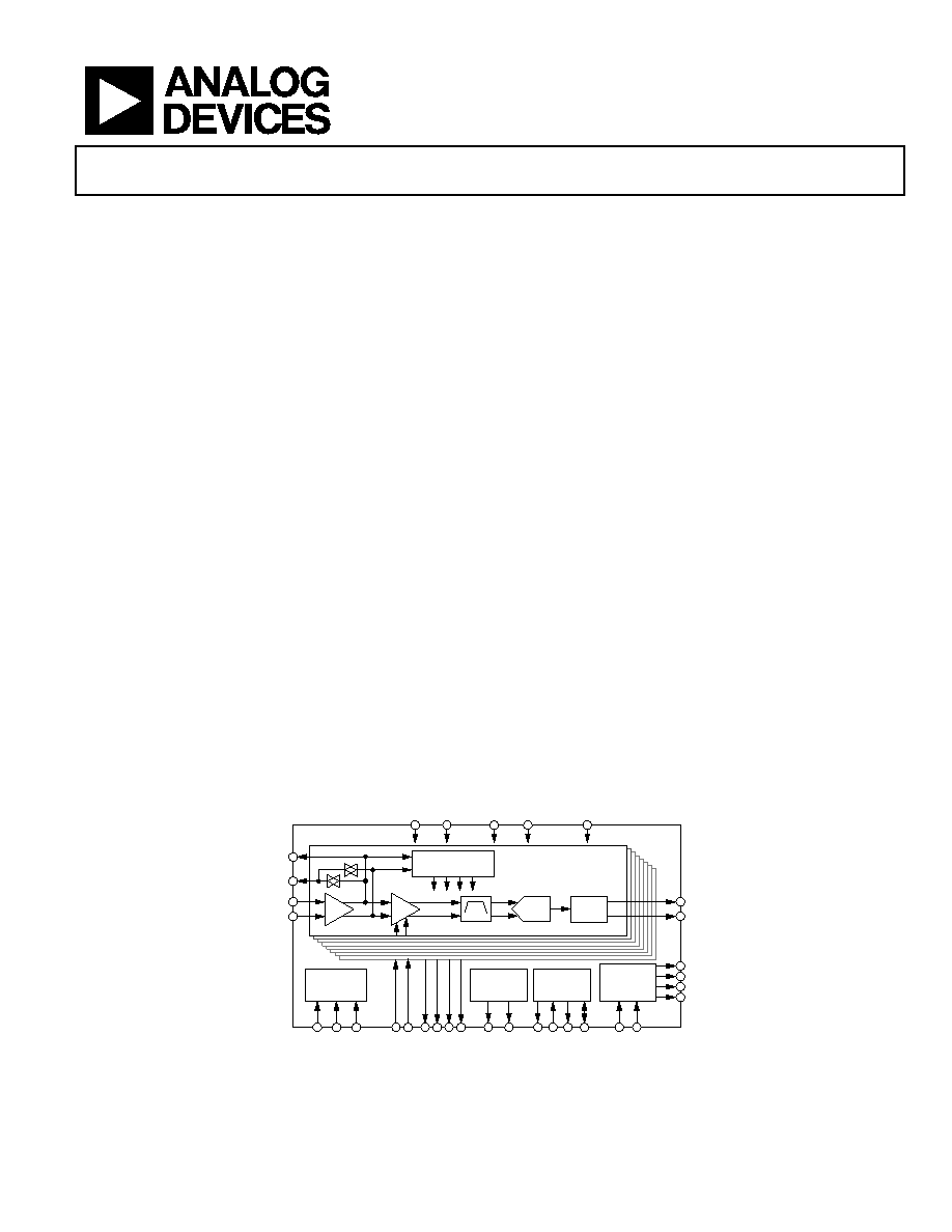
FUNCTIONAL BLOCK DIAGRAM
AAF
12-BIT
ADC
VGA
LNA
SERIAL
LVDS
I/Q
DEMODULATOR
8 CHANNELS
SERIAL
PORT
INTERFACE
DATA
RATE
MULTIPLIER
REFERENCE
LO
GENERATION
LO-A TO LO-H
LOSW-A TO LOSW-H
LI-A TO LI-H
LG-A TO LG-H
DOUTA+ TO DOUTH+
DOUTA– TO DOUTH–
FCO+
DRVDD
CL
K–
CL
K+
S
DI
O
S
CL
K
CS
B
G
PO
[0
:3
]
RBI
AS
VR
EF
CW
Q
+
CW
Q
–
CW
I+
CW
I–
G
AI
N–
G
AI
N+
4
LO–
4
LO+
R
ESET
STBY
PDWN
AVDD2
AVDD1
FCO–
DCO+
DCO–
09424-
001
Figure 1.
相关PDF资料 |
PDF描述 |
|---|---|
| AD9279BBCZ | IC ADC 12BIT 80MSPS 144CSPBGA |
| AD9393BBCZRL-80 | IC INTERFACE 80MHZ HDMI 76CSPBGA |
| AD9398KSTZ-150 | IC INTERFACE 150MHZ HDMI 100LQFP |
| AD9708ARU | IC DAC 8BIT 100MSPS 28-TSSOP |
| AD974BN | IC DAS 16BIT 4CH 200KSPS 28-DIP |
相关代理商/技术参数 |
参数描述 |
|---|---|
| AD9279 | 制造商:AD 制造商全称:Analog Devices 功能描述:Octal LNA/VGA/AAF/ADC and CW I/Q Demodulator |
| AD9279-65EBZ | 功能描述:BOARD EVALUATION FOR AD9279 RoHS:是 类别:编程器,开发系统 >> 评估板 - 模数转换器 (ADC) 系列:- 产品培训模块:Obsolescence Mitigation Program 标准包装:1 系列:- ADC 的数量:1 位数:12 采样率(每秒):94.4k 数据接口:USB 输入范围:±VREF/2 在以下条件下的电源(标准):- 工作温度:-40°C ~ 85°C 已用 IC / 零件:MAX11645 已供物品:板,软件 |
| AD9279-80KITZ | 功能描述:KIT EVALUATION FOR AD9279 RoHS:是 类别:编程器,开发系统 >> 评估板 - 模数转换器 (ADC) 系列:- 产品培训模块:Obsolescence Mitigation Program 标准包装:1 系列:- ADC 的数量:1 位数:12 采样率(每秒):94.4k 数据接口:USB 输入范围:±VREF/2 在以下条件下的电源(标准):- 工作温度:-40°C ~ 85°C 已用 IC / 零件:MAX11645 已供物品:板,软件 |
| AD9279BBCZ | 功能描述:IC ADC 12BIT 80MSPS 144CSPBGA RoHS:是 类别:集成电路 (IC) >> 数据采集 - ADCs/DAC - 专用型 系列:- 产品培训模块:Lead (SnPb) Finish for COTS Obsolescence Mitigation Program 标准包装:50 系列:- 类型:数据采集系统(DAS) 分辨率(位):16 b 采样率(每秒):21.94k 数据接口:MICROWIRE?,QSPI?,串行,SPI? 电压电源:模拟和数字 电源电压:1.8 V ~ 3.6 V 工作温度:-40°C ~ 85°C 安装类型:表面贴装 封装/外壳:40-WFQFN 裸露焊盘 供应商设备封装:40-TQFN-EP(6x6) 包装:托盘 |
| AD9279-BBCZ | 制造商:AD 制造商全称:Analog Devices 功能描述:Octal LNA/VGA/AAF/ADC and CW I/Q Demodulator |
发布紧急采购,3分钟左右您将得到回复。