参数资料
| 型号: | AD9515BCPZ |
| 厂商: | Analog Devices Inc |
| 文件页数: | 18/28页 |
| 文件大小: | 0K |
| 描述: | IC CLOCK DIST 2OUT PLL 32LFCSP |
| 设计资源: | Low Jitter Sampling Clock Generator for High Performance ADCs Using AD9958/9858 and AD9515 (CN0109) |
| 标准包装: | 1 |
| 类型: | 扇出缓冲器(分配),除法器 |
| PLL: | 无 |
| 输入: | 时钟 |
| 输出: | CMOS,LVDS,LVPECL |
| 电路数: | 1 |
| 比率 - 输入:输出: | 1:2 |
| 差分 - 输入:输出: | 是/是 |
| 频率 - 最大: | 1.6GHz |
| 除法器/乘法器: | 是/无 |
| 电源电压: | 3.135 V ~ 3.465 V |
| 工作温度: | -40°C ~ 85°C |
| 安装类型: | 表面贴装 |
| 封装/外壳: | 32-VFQFN 裸露焊盘,CSP |
| 供应商设备封装: | 32-LFCSP-VQ(5x5) |
| 包装: | 托盘 |
| 产品目录页面: | 776 (CN2011-ZH PDF) |
| 配用: | AD9515/PCBZ-ND - BOARD EVAL CLOCK 2CH AD9515 |
第1页第2页第3页第4页第5页第6页第7页第8页第9页第10页第11页第12页第13页第14页第15页第16页第17页当前第18页第19页第20页第21页第22页第23页第24页第25页第26页第27页第28页
Data Sheet
AD9515
Rev. A | Page 25 of 28
APPLICATIONS
USING THE AD9515 OUTPUTS FOR ADC CLOCK
APPLICATIONS
Any high speed, analog-to-digital converter (ADC) is extremely
sensitive to the quality of the sampling clock provided by the
user. An ADC can be thought of as a sampling mixer, and any
noise, distortion, or timing jitter on the clock is combined with
the desired signal at the A/D output. Clock integrity require-
ments scale with the analog input frequency and resolution,
with higher analog input frequency applications at ≥14-bit
resolution being the most stringent. The theoretical SNR of an
ADC is limited by the ADC resolution and the jitter on the
sampling clock. Considering an ideal ADC of infinite resolution
where the step size and quantization error can be ignored, the
available SNR can be expressed approximately by
×
=
J
ft
SNR
2π
1
log
20
where f is the highest analog frequency being digitized.
tj is the rms jitter on the sampling clock.
Figure 35 shows the required sampling clock jitter as a function
of the analog frequency and effective number of bits (ENOB).
fA FULL-SCALE SINE WAVE ANALOG FREQUENCY (MHz)
SNR
(dB)
ENOB
10
1k
100
30
40
50
60
70
80
90
100
110
6
8
10
12
14
16
18
T
J = 100
f
S
200
f
S
400
f
S
1ps
2ps
10ps
SNR = 20log
1
2
πf
ATJ
05597-091
Figure 35. ENOB and SNR vs. Analog Input Frequency
See Application Notes AN-756 and AN-501 at www.analog.com.
Many high performance ADCs feature differential clock inputs
to simplify the task of providing the required low jitter clock on
a noisy PCB. (Distributing a single-ended clock on a noisy PCB
can result in coupled noise on the sample clock. Differential
distribution has inherent common-mode rejection that can
provide superior clock performance in a noisy environment.)
The AD9515 features both LVPECL and LVDS outputs that
provide differential clock outputs, which enable clock solutions
that maximize converter SNR performance. The input
requirements of the ADC (differential or single-ended, logic
level, termination) should be considered when selecting the best
clocking/converter solution.
LVPECL CLOCK DISTRIBUTION
The low voltage, positive emitter-coupled, logic (LVPECL)
outputs of the AD9515 provide the lowest jitter clock signals
available from the AD9515. The LVPECL outputs (because they
are open emitter) require a dc termination to bias the output
transistors. The simplified equivalent circuit in Figure 31 shows
the LVPECL output stage.
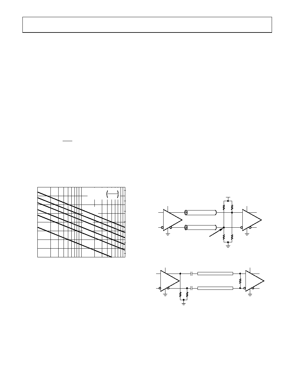
In most applications, a standard LVPECL far-end termination is
recommended, as shown in Figure 36. The resistor network is
designed to match the transmission line impedance (50 ) and
the switching threshold (VS 1.3 V).
VS
LVPECL
50
50
SINGLE-ENDED
(NOT COUPLED)
VS
LVPECL
127
127
83
83
VT = VS – 1.3V
05597-030
Figure 36. LVPECL Far-End Termination
VS
LVPECL
100
DIFFERENTIAL
(COUPLED)
VS
LVPECL
100
0.1nF
200
200
05597-031
Figure 37. LVPECL with Parallel Transmission Line
相关PDF资料 |
PDF描述 |
|---|---|
| VE-JVV-MZ-S | CONVERTER MOD DC/DC 5.8V 25W |
| SY58025UMG TR | IC MUX DUAL 2:1 CML PREC 32-MLF |
| AD9513BCPZ | IC CLOCK DIST 3OUT PLL 32LFCSP |
| SY10E167JZ | IC MUX/REGISTER 6BIT 2:1 28PLCC |
| AD9572ACPZLVD | IC PLL CLOCK GEN 25MHZ 40LFCSP |
相关代理商/技术参数 |
参数描述 |
|---|---|
| AD9515BCPZ-REEL7 | 功能描述:IC CLOCK DIST 2OUT PLL 32LFCSP RoHS:是 类别:集成电路 (IC) >> 时钟/计时 - 时钟发生器,PLL,频率合成器 系列:- 标准包装:1,000 系列:Precision Edge® 类型:时钟/频率合成器 PLL:无 输入:CML,PECL 输出:CML 电路数:1 比率 - 输入:输出:2:1 差分 - 输入:输出:是/是 频率 - 最大:10.7GHz 除法器/乘法器:无/无 电源电压:2.375 V ~ 3.6 V 工作温度:-40°C ~ 85°C 安装类型:表面贴装 封装/外壳:16-VFQFN 裸露焊盘,16-MLF? 供应商设备封装:16-MLF?(3x3) 包装:带卷 (TR) 其它名称:SY58052UMGTRSY58052UMGTR-ND |
| AD95160 | 制造商:AD 制造商全称:Analog Devices 功能描述:14-Channel Clock Generator with Integrated 2.8 GHz VCO |
| AD9516-0 | 制造商:AD 制造商全称:Analog Devices 功能描述:14-Output Clock Generator with Integrated 2.8 GHz VCO |
| AD9516-0/PCBZ | 功能描述:IC CLOCK GEN 2.8GHZ VCO 64-LFCSP RoHS:是 类别:编程器,开发系统 >> 评估演示板和套件 系列:- 标准包装:1 系列:- 主要目的:电信,线路接口单元(LIU) 嵌入式:- 已用 IC / 零件:IDT82V2081 主要属性:T1/J1/E1 LIU 次要属性:- 已供物品:板,电源,线缆,CD 其它名称:82EBV2081 |
| AD9516-0_07 | 制造商:AD 制造商全称:Analog Devices 功能描述:14-Output Clock Generator with Integrated 2.8 GHz VCO |
发布紧急采购,3分钟左右您将得到回复。