- 您现在的位置:买卖IC网 > PDF目录16533 > AD9517-2A/PCBZ (Analog Devices Inc)BOARD EVALUATION FOR AD9517-2A PDF资料下载
参数资料
| 型号: | AD9517-2A/PCBZ |
| 厂商: | Analog Devices Inc |
| 文件页数: | 43/80页 |
| 文件大小: | 0K |
| 描述: | BOARD EVALUATION FOR AD9517-2A |
| 设计资源: | AD9517 Eval Brd Schematics AD9517 Gerber Files AD9517-2 BOM |
| 标准包装: | 1 |
| 主要目的: | 计时,时钟发生器 |
| 嵌入式: | 否 |
| 已用 IC / 零件: | AD9517-2A |
| 主要属性: | 2 输入,12 输出,2.2GHz VCO |
| 次要属性: | CMOS,LVPECL 和 LVDS 兼容 |
| 已供物品: | 板 |
第1页第2页第3页第4页第5页第6页第7页第8页第9页第10页第11页第12页第13页第14页第15页第16页第17页第18页第19页第20页第21页第22页第23页第24页第25页第26页第27页第28页第29页第30页第31页第32页第33页第34页第35页第36页第37页第38页第39页第40页第41页第42页当前第43页第44页第45页第46页第47页第48页第49页第50页第51页第52页第53页第54页第55页第56页第57页第58页第59页第60页第61页第62页第63页第64页第65页第66页第67页第68页第69页第70页第71页第72页第73页第74页第75页第76页第77页第78页第79页第80页
AD9517-2
Data Sheet
Rev. E | Page 48 of 80
12
3
4
5
6
7
8
910
INPUT TO VCO DIVIDER
INPUT TO CHANNEL DIVIDER
OUTPUT OF
CHANNEL DIVIDER
SYNC PIN
1
11
12
13
14
14 TO 15 CYCLES AT CHANNEL DIVIDER INPUT + 1 CYCLE AT VCO DIVIDER INPUT
CHANNEL DIVIDER OUTPUT STATIC
CHANNEL DIVIDER
OUTPUT CLOCKING
CHANNEL DIVIDER
OUTPUT CLOCKING
06
42
6-
0
73
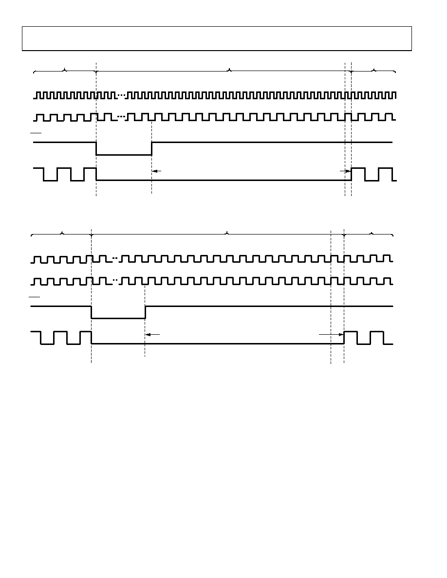
Figure 57. SYNC Timing When VCO Divider Is Used—CLK or VCO Is Input
INPUT TO CLK
IINPUT TO CHANNEL DIVIDER
OUTPUT OF
CHANNEL DIVIDER
SYNC PIN
14 TO 15 CYCLES AT CHANNEL DIVIDER INPUT + 1 CYCLE AT CLK INPUT
12
3
4
5
6
7
8
910
11
12
13
14
1
CHANNEL DIVIDER OUTPUT STATIC
CHANNEL DIVIDER
OUTPUT CLOCKING
CHANNEL DIVIDER
OUTPUT CLOCKING
0
6
426
-07
4
Figure 58. SYNC Timing When VCO Divider Is Not Used—CLK Input Only
A sync operation brings all outputs that have not been excluded
(by the nosync bit) to a preset condition before allowing the
outputs to begin clocking in synchronicity. The preset condition
takes into account the settings in each of the channel’s start high
bit and its phase offset. These settings govern both the static
state of each output when the sync operation is happening and
the state and relative phase of the outputs when they begin clocking
again upon completion of the sync operation. Between outputs
and after synchronization, this allows for the setting of phase
offsets.
The AD9517 outputs are in pairs, sharing a channel divider per
pair (two pairs of pairs, four outputs, in the case of CMOS). The
synchronization conditions apply to both outputs of a pair.
Each channel (a divider and its outputs) can be excluded from
any sync operation by setting the nosync bit of the channel.
Channels that are set to ignore SYNC (excluded channels) do
not set their outputs static during a sync operation, and their
outputs are not synchronized with those of the nonexcluded
channels.
Clock Outputs
The AD9517 offers three different output level choices:
LVPECL, LVDS, and CMOS. OUT0 to OUT3 are LVPECL
differential outputs; and OUT4 to OUT7 are LVDS/CMOS
outputs. These outputs can be configured as either LVDS
differential or as pairs of single-ended CMOS outputs.
相关PDF资料 |
PDF描述 |
|---|---|
| VI-J00-EZ-S | CONVERTER MOD DC/DC 5V 25W |
| ILC0402ER15NK | INDUCTOR CER 15NH 0402 |
| SP1210R-473K | INDUCTOR PWR SHIELDED 47.0UH SMD |
| MCP121T-300E/TT | IC SUPERVISOR 2.93V LOW SOT-23B |
| AD9517-4A/PCBZ | BOARD EVALUATION FOR AD9517-4A |
相关代理商/技术参数 |
参数描述 |
|---|---|
| AD9517-2BCPZ | 制造商:Analog Devices 功能描述:Clock Generator 48-Pin LFCSP EP Tray |
| AD9517-2BCPZ-REEL7 | 制造商:Analog Devices 功能描述: |
| AD9517-2BCPZ-TR | 制造商:Analog Devices 功能描述:OUPUT CLOCK GENERATOR WITH 2.2HZ VCO - Tape and Reel |
| AD9517-3 | 制造商:AD 制造商全称:Analog Devices 功能描述:12-Output Clock Generator with Integrated 2.0 GHz VCO |
| AD9517-3A/PCBZ | 功能描述:BOARD EVALUATION FOR AD9517-3A RoHS:是 类别:编程器,开发系统 >> 评估演示板和套件 系列:- 标准包装:1 系列:PSoC® 主要目的:电源管理,热管理 嵌入式:- 已用 IC / 零件:- 主要属性:- 次要属性:- 已供物品:板,CD,电源 |
发布紧急采购,3分钟左右您将得到回复。