- 您现在的位置:买卖IC网 > PDF目录16534 > AD9518-4A/PCBZ (Analog Devices Inc)BOARD EVALUATION FOR AD9518-4A PDF资料下载
参数资料
| 型号: | AD9518-4A/PCBZ |
| 厂商: | Analog Devices Inc |
| 文件页数: | 6/64页 |
| 文件大小: | 0K |
| 描述: | BOARD EVALUATION FOR AD9518-4A |
| 设计资源: | AD9518 Schematics AD9518 Gerber Files AD9518-4 BOM |
| 标准包装: | 1 |
| 主要目的: | 计时,时钟发生器 |
| 嵌入式: | 否 |
| 已用 IC / 零件: | AD9518-4A |
| 主要属性: | 2 输入,14 输出,1.6GHz VCO |
| 次要属性: | LVPECL 输出逻辑 |
| 已供物品: | 板 |
第1页第2页第3页第4页第5页当前第6页第7页第8页第9页第10页第11页第12页第13页第14页第15页第16页第17页第18页第19页第20页第21页第22页第23页第24页第25页第26页第27页第28页第29页第30页第31页第32页第33页第34页第35页第36页第37页第38页第39页第40页第41页第42页第43页第44页第45页第46页第47页第48页第49页第50页第51页第52页第53页第54页第55页第56页第57页第58页第59页第60页第61页第62页第63页第64页
AD9518-4
Data Sheet
Rev. B | Page 14 of 64
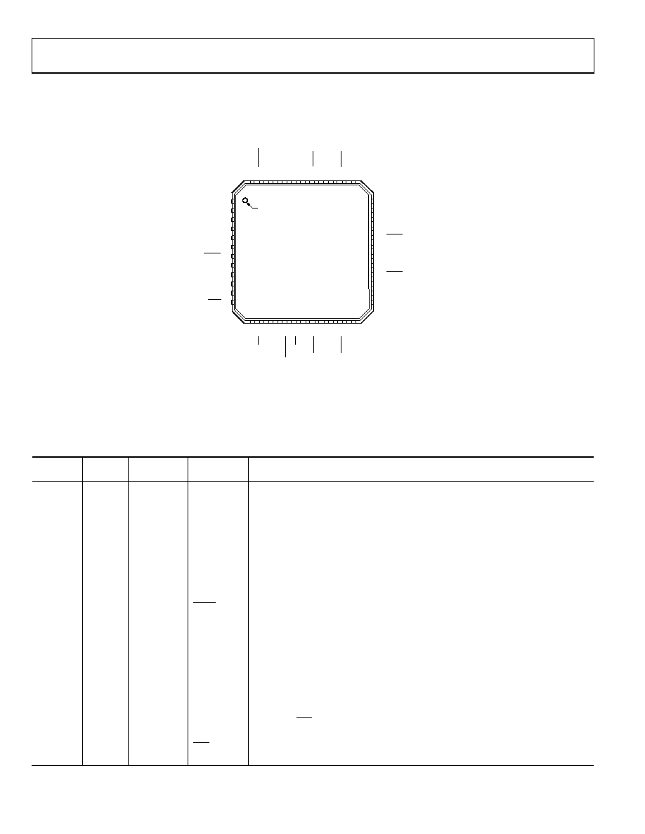
PIN CONFIGURATION AND FUNCTION DESCRIPTIONS
13
14
15
16
17
18
19
20
21
22
23
24
SC
L
K
CS
SD
O
SD
IO
R
E
SET
PD
OU
T
4
OU
T
4
VS
_L
VP
E
C
L
OU
T
5
OU
T
5
VS
48
47
46
45
44
43
42
41
40
39
38
37
RE
F
IN
(
R
E
F
1)
RE
F
IN
(
R
E
F
2)
CP
RS
E
T
VS
RS
E
T
VS
OU
T0
OU
T0
VS
_L
VP
EC
L
OU
T1
OU
T1
VS
1
2
3
4
5
6
7
8
9
10
11
12
35
36
34
33
32
31
30
29
28
27
26
25
AD9518-4
TOP VIEW
(Not to Scale)
PIN 1
INDICATOR
CP
STATUS
CLK
VCP
REFMON
LD
BYPASS
VS
REF_SEL
LF
SYNC
CLK
OUT3
OUT2
VS
VS_LVPECL
OUT3
OUT2
NC
GND
VS
GND
06
43
3-
0
03
NOTES
1. NC = NO CONNECT.
2. THE EXTERNAL PADDLE ON THE BOTTOM OF THE PACKAGE MUST BE
CONNECTED TO GROUND FOR PROPER OPERATION.
Figure 4. Pin Configuration
Table 19. Pin Function Descriptions
Pin No.
Input/
Output
Pin Type
Mnemonic
Description
1
I
3.3 V CMOS
REFMON
Reference Monitor (Output). This pin has multiple selectable outputs; see Table 44,
Register 0x01B.
2
O
3.3 V CMOS
LD
Lock Detect (Output). This pin has multiple selectable outputs; see Table 44,
Register 0x01A.
3
I
Power
VCP
Power Supply for Charge Pump (CP). VS ≤ VCP ≤ 5.0 V. This pin is usually 3.3 V for most
applications; but if a 5 V external VCXO is used, this pin should be 5 V.
4
O
CP
Charge Pump (Output). Connects to external loop filter.
5
O
3.3 V CMOS
STATUS
Status (Output). This pin has multiple selectable outputs; see Table 44, Register 0x017.
6
I
3.3 V CMOS
REF_SEL
Reference Select. Selects REF1 (low) or REF2 (high). This pin has an internal 30 kΩ
pull-down resistor.
7
I
3.3 V CMOS
SYNC
Manual Synchronizations and Manual Holdover. This pin initiates a manual
synchronization and is also used for manual holdover. Active low. This pin has an
internal 30 kΩ pull-up resistor.
8
I
Loop filter
LF
Loop Filter (Input). Connects to VCO control voltage node internally. This pin has 31 pF of
internal capacitance to ground, which may influence the loop filter design for large
loop bandwidths.
9
O
Loop filter
BYPASS
This pin is for bypassing the LDO to ground with a capacitor.
10, 24, 25,
26, 35, 37,
43, 45
I
Power
VS
3.3 V Power Pins.
Along with CLK, this is the self-biased differential input for the clock distribution section.
This pin can be left floating if internal VCO is used.
11
I
Differential
clock input
CLK
12
I
Differential
clock input
CLK
Along with CLK, this is the self-biased differential input for the clock distribution section.
This pin can be left floating if internal VCO is used.
相关PDF资料 |
PDF描述 |
|---|---|
| BA6920FP-Y | IC DRIVER REVERSE MOTOR HSOP25 |
| VE-JTW-EZ-S | CONVERTER MOD DC/DC 5.5V 25W |
| AD9518-2A/PCBZ | BOARD EVALUATION FOR AD9518-2A |
| FCBP110LD1L10 | CABLE 10.5GBPS 10M LASERWIRE |
| ADCLK946/PCBZ | KIT EVAL CLK BUFF ADCLK946 |
相关代理商/技术参数 |
参数描述 |
|---|---|
| AD9518-4BCPZ | 制造商:Rochester Electronics LLC 功能描述: 制造商:Analog Devices 功能描述: |
| AD9518-4BCPZ-REEL7 | 制造商:Analog Devices 功能描述: |
| AD9520 | 制造商:AD 制造商全称:Analog Devices 功能描述:Synchronizing Multiple AD9910 1 GSPS Direct Digital Synthesizers |
| AD9520-0 | 制造商:AD 制造商全称:Analog Devices 功能描述:12 LVPECL/24 CMOS Output Clock Generator with Integrated 2.8 GHz VCO |
| AD9520-0/PCBZ | 功能描述:BOARD EVAL AD9520-0 RoHS:是 类别:编程器,开发系统 >> 评估演示板和套件 系列:- 标准包装:1 系列:PSoC® 主要目的:电源管理,热管理 嵌入式:- 已用 IC / 零件:- 主要属性:- 次要属性:- 已供物品:板,CD,电源 |
发布紧急采购,3分钟左右您将得到回复。