参数资料
| 型号: | AD9523-1BCPZ |
| 厂商: | Analog Devices Inc |
| 文件页数: | 24/60页 |
| 文件大小: | 0K |
| 描述: | IC INTEGER-N CLCK GEN 72LFCSP |
| 标准包装: | 1 |
| 类型: | 时钟/频率发生器,扇出缓冲器(分配),多路复用器 |
| PLL: | 是 |
| 主要目的: | 以太网,光纤通道,SONET/SDH |
| 输入: | CMOS |
| 输出: | HSTL,LVCMOS,LVDS,LVPECL |
| 电路数: | 1 |
| 比率 - 输入:输出: | 2:14 |
| 差分 - 输入:输出: | 是/是 |
| 频率 - 最大: | 1GHz |
| 电源电压: | 1.768 V ~ 3.465 V |
| 工作温度: | -40°C ~ 85°C |
| 安装类型: | 表面贴装 |
| 封装/外壳: | 72-VFQFN 裸露焊盘,CSP |
| 供应商设备封装: | 72-LFCSP |
| 包装: | 托盘 |
| 配用: | AD9523/PCBZ-ND - BOARD EVAL FOR AD9523 |
第1页第2页第3页第4页第5页第6页第7页第8页第9页第10页第11页第12页第13页第14页第15页第16页第17页第18页第19页第20页第21页第22页第23页当前第24页第25页第26页第27页第28页第29页第30页第31页第32页第33页第34页第35页第36页第37页第38页第39页第40页第41页第42页第43页第44页第45页第46页第47页第48页第49页第50页第51页第52页第53页第54页第55页第56页第57页第58页第59页第60页
AD9523-1
Rev. B | Page 30 of 60
A repeated start (Sr) condition can be used in place of a stop
condition. Furthermore, a start or stop condition can occur at
any time; partially transferred bytes are discarded.
For an I2C data write transfer containing multiple data bytes,
the peripheral drives a no acknowledge for the data byte that
follows a write to Register 0x234, thereby ending the I2C transfer.
For an I2C data read transfer containing multiple data bytes,
the peripheral drives data bytes of 0x00 for subsequent reads that
follow a read from Register 0x234.
Data Transfer Format
Send byte format. The send byte protocol is used to set up the register address for subsequent commands.
S
Slave Address
W
A
RAM Address High Byte
A
RAM Address Low Byte
A
P
Write byte format. The write byte protocol is used to write a register address to the RAM, starting from the specified RAM address.
S
Slave Address
W
A
RAM Address
High Byte
A
RAM Address
Low Byte
A
RAM
Data 0
A
RAM
Data 1
A
RAM
Data 2
A
P
Receive byte format. The receive byte protocol is used to read the data byte(s) from the RAM, starting from the current address.
S
Slave Address
R
A
RAM Data 0
A
RAM Data 1
A
RAM Data 2
A
P
Read byte format. The combined format of the send byte and the receive byte.
S
Slave
Address
W
A
RAM Address
High Byte
A
RAM Address
Low Byte
A
Sr
Slave
Address
R
A
RAM
Data 0
A
RAM
Data 1
A
RAM
Data 2
A
P
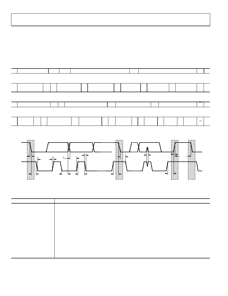
IC Serial Port Timing
SDA
SCL
S
Sr
P
S
tFALL
tSET; DAT
tLOW
tRISE
tHLD; STR
tHLD; DAT
tHIGH
tFALL
tSET; STR
tHLD; STR
tSPIKE
tSET; STP
tRISE
tIDLE
09278
-1
65
Figure 37. IC Serial Port Timing
Table 23. I2C Timing Definitions
Parameter
Description
fI2C
IC clock frequency
tIDLE
Bus idle time between stop and start conditions
tHLD; STR
Hold time for repeated start condition
tSET; STR
Setup time for repeated start condition
tSET; STP
Setup time for stop condition
tHLD; DAT
Hold time for data
tSET; DAT
Setup time for data
tLOW
Duration of SCL clock low
tHIGH
Duration of SCL clock high
tRISE
SCL/SDA rise time
tFALL
SCL/SDA fall time
tSPIKE
Voltage spike pulse width that must be suppressed by the input filter
相关PDF资料 |
PDF描述 |
|---|---|
| ATA6620-TAQY | IC TXRX LIN BUS 5V/50MA 8SOIC |
| SM843001-106KA | IC CLK SYNTHESIZER FIBRE 8-TSSOP |
| SM840002KA | IC CLK SYNTHESIZER LN 16-TSSOP |
| V150B15M150BL | CONVERTER MOD DC/DC 15V 150W |
| MS3102R32-15S | CONN RCPT 8POS BOX MNT W/SCKT |
相关代理商/技术参数 |
参数描述 |
|---|---|
| AD9523-1BCPZ-REEL7 | 功能描述:IC INTEGER-N CLCK GEN 72LFCSP RoHS:是 类别:集成电路 (IC) >> 时钟/计时 - 专用 系列:- 标准包装:28 系列:- 类型:时钟/频率发生器 PLL:是 主要目的:Intel CPU 服务器 输入:时钟 输出:LVCMOS 电路数:1 比率 - 输入:输出:3:22 差分 - 输入:输出:无/是 频率 - 最大:400MHz 电源电压:3.135 V ~ 3.465 V 工作温度:0°C ~ 85°C 安装类型:表面贴装 封装/外壳:64-TFSOP (0.240",6.10mm 宽) 供应商设备封装:64-TSSOP 包装:管件 |
| AD9523BCPZ | 功能描述:IC INTEGER-N CLCK GEN 72LFCSP RoHS:是 类别:集成电路 (IC) >> 时钟/计时 - 专用 系列:- 标准包装:28 系列:- 类型:时钟/频率发生器 PLL:是 主要目的:Intel CPU 服务器 输入:时钟 输出:LVCMOS 电路数:1 比率 - 输入:输出:3:22 差分 - 输入:输出:无/是 频率 - 最大:400MHz 电源电压:3.135 V ~ 3.465 V 工作温度:0°C ~ 85°C 安装类型:表面贴装 封装/外壳:64-TFSOP (0.240",6.10mm 宽) 供应商设备封装:64-TSSOP 包装:管件 |
| AD9523BCPZ-REEL7 | 功能描述:IC INTEGER-N CLCK GEN 72LFCSP RoHS:是 类别:集成电路 (IC) >> 时钟/计时 - 专用 系列:- 标准包装:28 系列:- 类型:时钟/频率发生器 PLL:是 主要目的:Intel CPU 服务器 输入:时钟 输出:LVCMOS 电路数:1 比率 - 输入:输出:3:22 差分 - 输入:输出:无/是 频率 - 最大:400MHz 电源电压:3.135 V ~ 3.465 V 工作温度:0°C ~ 85°C 安装类型:表面贴装 封装/外壳:64-TFSOP (0.240",6.10mm 宽) 供应商设备封装:64-TSSOP 包装:管件 |
| AD9524 | 制造商:AD 制造商全称:Analog Devices 功能描述:Jitter Cleaner and Clock Generator with 6 Differential or 13 LVCMOS Outputs |
| AD9524/PCBZ | 功能描述:BOARD EVAL FOR AD9524 RoHS:是 类别:编程器,开发系统 >> 评估演示板和套件 系列:- 标准包装:1 系列:PSoC® 主要目的:电源管理,热管理 嵌入式:- 已用 IC / 零件:- 主要属性:- 次要属性:- 已供物品:板,CD,电源 |
发布紧急采购,3分钟左右您将得到回复。