参数资料
| 型号: | AD9550/PCBZ |
| 厂商: | Analog Devices Inc |
| 文件页数: | 1/8页 |
| 文件大小: | 0K |
| 描述: | BOARD EVALUATION FOR AD9550 |
| 标准包装: | 1 |
| 主要目的: | 计时,时钟缓冲器 / 驱动器 / 接收器 / 变换器 |
| 嵌入式: | 否 |
| 已用 IC / 零件: | AD9550 |
| 主要属性: | 1 输入,2 输出 |
| 次要属性: | CMOS,LVPECL 和 LVDS 兼容 |
| 已供物品: | 板 |
�� �����
�����
�����Evaluation� Board� User� Guide�
�UG-203�
�One� Technology� Way� ?� P.O.� Box� 9106� ?� Norwood,� MA� 02062-9106,� U.S.A.� ?� Tel:� 781.329.4700� ?� Fax:� 781.461.3113� ?� www.analog.com�
�Evaluating� the� AD9550� Integer-N� Clock� Translator�
�FEATURES�
�Converts� preset� standard� input� frequencies� to� standard�
�output� frequencies�
�Input� frequencies� from� 8� kHz� to� 200� MHz�
�Output� frequencies� up� to� 810� MHz� LVPECL� and� LVDS�
�(200� MHz� CMOS)�
�Preset� pin-programmable� frequency� translation� ratios�
�On-chip� VCO�
�Single-ended� CMOS� reference� input�
�2� output� clocks� (independently� programmable� as� LVDS,�
�LVPECL,� or� CMOS)�
�Single� supply� (3.3� V)�
�Very� low� power:� <450� mW� (under� most� conditions)�
�Small� package� size:� 5� mm� � 5� mm�
�Exceeds� Telcordia� GR-253-CORE� jitter� generation,� transfer�
�and� tolerance� specifications�
�APPLICATIONS�
�Cost� effective� replacement� of� high� frequency� VCXO,� OCXO,�
�and� SAW� resonators�
�Flexible� frequency� translation� for� wireline� applications� such�
�as� Ethernet,� T1/E1,� SONET/SDH,� GPON,� xDSL�
�GENERAL� DESCRIPTION�
�This� user� guide� describes� the� hardware� of� the� AD9550� eval-�
�uation� board.� The� AD9550� evaluation� board� is� a� compact,�
�easy-to-use� platform� for� evaluating� all� features� of� the� AD9550�
�integer-N� clock� translator.�
�The� AD9550� is� a� phase-locked� loop� (PLL)� based� clock� trans-�
�lator� designed� to� address� the� needs� of� wireline� communication�
�and� base� station� applications.� The� device� employs� an� integer-N�
�PLL� to� accommodate� the� applicable� frequency� translation�
�requirements.� It� accepts� a� single-ended� input� reference� signal�
�at� the� REF� input.�
�The� AD9550� is� pin� programmable,� providing� a� matrix� of�
�standard� input/output� frequency� translations� from� a� list� of�
�15� possible� input� frequencies� to� a� list� of� 52� possible� output�
�frequency� pairs� (OUT1� and� OUT2).�
�The� AD9550� output� is� compatible� with� LVPECL,� LVDS,� or�
�single-ended� CMOS� logic� levels,� although� the� AD9550� is�
�implemented� in� a� strictly� CMOS� process.�
�The� AD9550� operates� over� the� extended� industrial� temperature�
�range� of� ?40°C� to� +85°C.�
�Wireless� infrastructure�
�Test� and� measurement� (including� handheld� devices)�
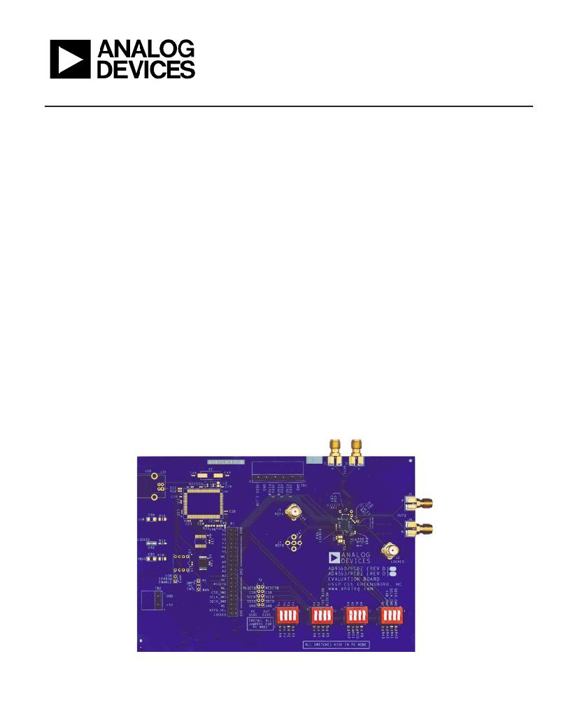
�DIGITAL� PICTURE� OF� THE� AD9550� EVALUATION� BOARD�
�Figure� 1.� AD9550� Evaluation� Board�
�PLEASE� SEE� THE� LAST� PAGE� FOR� AN� IMPORTANT�
�WARNING� AND� LEGAL� TERMS� AND� CONDITIONS.�
�Rev.� 0� |� Page� 1� of� 8�
�相关PDF资料 |
PDF描述 |
|---|---|
| AD9985A/PCBZ | KIT EVALUATION FOR AD9985A |
| ADA4850-2YCP-EBZ | BOARD EVAL FOR ADA4850-2YCP |
| ADA4899-1YCP-EBZ | BOARD EVAL FOR ADA4899-1YCP |
| ADA4937-1YCP-EBZ | BOARD EVAL FOR ADA4937-1YCP |
| ADA4938-2YCP-EBZ | BOARD EVAL FOR ADA4938-2YCP |
相关代理商/技术参数 |
参数描述 |
|---|---|
| AD9551 | 制造商:AD 制造商全称:Analog Devices 功能描述:Multiservice Clock Generator |
| AD9551/PCBZ | 功能描述:BOARD EVAL FOR AD9951 RoHS:是 类别:编程器,开发系统 >> 评估演示板和套件 系列:- 标准包装:1 系列:PSoC® 主要目的:电源管理,热管理 嵌入式:- 已用 IC / 零件:- 主要属性:- 次要属性:- 已供物品:板,CD,电源 |
| AD9551BCPZ | 功能描述:IC CLOCK GEN MULTISERV 40-LFCSP RoHS:是 类别:集成电路 (IC) >> 时钟/计时 - 时钟发生器,PLL,频率合成器 系列:- 标准包装:2,000 系列:- 类型:PLL 时钟发生器 PLL:带旁路 输入:LVCMOS,LVPECL 输出:LVCMOS 电路数:1 比率 - 输入:输出:2:11 差分 - 输入:输出:是/无 频率 - 最大:240MHz 除法器/乘法器:是/无 电源电压:3.135 V ~ 3.465 V 工作温度:0°C ~ 70°C 安装类型:表面贴装 封装/外壳:32-LQFP 供应商设备封装:32-TQFP(7x7) 包装:带卷 (TR) |
| AD9551BCPZ-REEL7 | 功能描述:IC CLOCK GEN TRANSLATOR 40LFCSP RoHS:是 类别:集成电路 (IC) >> 时钟/计时 - 时钟发生器,PLL,频率合成器 系列:- 标准包装:2,000 系列:- 类型:PLL 时钟发生器 PLL:带旁路 输入:LVCMOS,LVPECL 输出:LVCMOS 电路数:1 比率 - 输入:输出:2:11 差分 - 输入:输出:是/无 频率 - 最大:240MHz 除法器/乘法器:是/无 电源电压:3.135 V ~ 3.465 V 工作温度:0°C ~ 70°C 安装类型:表面贴装 封装/外壳:32-LQFP 供应商设备封装:32-TQFP(7x7) 包装:带卷 (TR) |
| AD9552 | 制造商:AD 制造商全称:Analog Devices 功能描述:Oscillator Frequency Upconverter |
发布紧急采购,3分钟左右您将得到回复。