- 您现在的位置:买卖IC网 > PDF目录9093 > AD9571ACPZPEC-RL (Analog Devices Inc)IC PLL CLOCK GEN 25MHZ 40LFCSP PDF资料下载
参数资料
| 型号: | AD9571ACPZPEC-RL |
| 厂商: | Analog Devices Inc |
| 文件页数: | 7/20页 |
| 文件大小: | 0K |
| 描述: | IC PLL CLOCK GEN 25MHZ 40LFCSP |
| 标准包装: | 2,500 |
| 类型: | 时钟发生器,扇出配送,多路复用器 |
| PLL: | 是 |
| 输入: | 晶体 |
| 输出: | CMOS,LVDS,LVPECL |
| 电路数: | 1 |
| 比率 - 输入:输出: | 1:10 |
| 差分 - 输入:输出: | 无/是 |
| 频率 - 最大: | 156.25MHz |
| 除法器/乘法器: | 是/无 |
| 电源电压: | 2.97 V ~ 3.63 V |
| 工作温度: | -40°C ~ 85°C |
| 安装类型: | 表面贴装 |
| 封装/外壳: | 40-WFQFN 裸露焊盘,CSP |
| 供应商设备封装: | 40-LFCSP-WQ(6x6) |
| 包装: | 带卷 (TR) |
AD9571
Rev. 0 | Page 15 of 20
Table 15. FREQSEL Definition
FREQSEL
Frequency Available
from Pin 19 and Pin 20
(MHZ)
Frequency Available
from Pin 21 and Pin 22
(MHZ)
0
125
1
100
NC
125
100
3.5mA
OUT
07499-
012
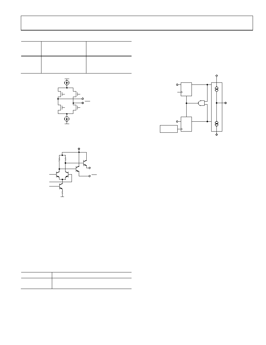
Figure 12. LVDS Output Simplified Equivalent Circuit
The simplified equivalent circuits of the LVDS and LVPECL
outputs are shown in Figure 12 and Figure 13.
3.3V
OUT
GND
07499-
013
Figure 13. LVPECL Output Simplified Equivalent Circuit
The differential outputs are factory programmed to either LVPECL
or LVDS format, and either option can be sampled on request.
CMOS drivers tend to generate more noise than differential
outputs and, as a result, the proximity of the 33.33 MHz output
to Pin 21 and Pin 22 does affect the jitter performance when
FREQSEL = 0 (that is, when the differential output is generating
125 MHz). For this reason, the 33.33 MHz pin can be forced to
a low state by asserting the FORCE_LOW signal on Pin 37 (see
Table 16). An internal pull-down enables the 33.33 MHz output
if the pin is not connected.
Table 16. FORCE_LOW (Pin 37) Definition
FORCE_LOW
33.33 MHz Output (Pin 23)
0 or NC
33.33 MHz
1
0 MHz
PHASE FREQUENCY DETECTOR (PFD) AND
CHARGE PUMP
The PFD takes inputs from the reference clock and feedback
divider to produce an output proportional to the phase and
frequency difference between them. Figure 14 shows a
simplified schematic.
D1
Q1
CLR1
REFCLK
HIGH
UP
D2
Q2
CLR2
HIGH
DOWN
CP
CHARGE
PUMP
3.3V
GND
FEEDBACK
DIVIDER
07499-
014
Figure 14. PFD Simplified Schematic
POWER SUPPLY
The AD9571 requires a 3.3 V ± 10% power supply for VS. The
Specifications section gives the performance expected from the
AD9571 with the power supply voltage within this range. The
absolute maximum range of (0.3 V) (+3.6 V), with respect to
GND, must never be exceeded on the VS pin.
Good engineering practice should be followed in the layout of
power supply traces and the ground plane of the PCB. Bypass
the power supply on the PCB with adequate capacitance (>10
F). Bypass the AD9571 with adequate capacitors (0.1 F) at all
power pins as close as possible to the part. The layout of the
AD9571 evaluation board is a good example.
The exposed metal paddle on the AD9571 package is an electrical
connection, as well as a thermal enhancement. For the device to
function properly, the paddle must be properly attached to ground
(GND). The PCB acts as a heat sink for the AD9571; therefore,
this GND connection should provide a good thermal path to a
larger dissipation area, such as a ground plane on the PCB.
CMOS CLOCK DISTRIBUTION
The AD9571 provides seven CMOS clock outputs (six 25 MHz
and one 33.33 MHz) that are dedicated CMOS levels. Whenever
single-ended CMOS clocking is used, some of the following
general guidelines should be followed.
Point-to-point nets should be designed such that a driver has
one receiver only on the net, if possible. This allows for simple
termination schemes and minimizes ringing due to possible
mismatched impedances on the net. Series termination at the
source is generally required to provide transmission line
matching and/or to reduce current transients at the driver.
相关PDF资料 |
PDF描述 |
|---|---|
| MS27508E24F2PA | CONN RCPT 100POS BOX MNT W/PINS |
| MS27508E24B2PA | CONN RCPT 100POS BOX MNT W/PINS |
| X9410WP24-2.7 | IC XDCP DUAL 64-TAP 10K 24-DIP |
| VE-BTL-MV-S | CONVERTER MOD DC/DC 28V 150W |
| AD9572ACPZLVD-RL | IC PLL CLOCK GEN 25MHZ 40LFCSP |
相关代理商/技术参数 |
参数描述 |
|---|---|
| AD9572 | 制造商:AD 制造商全称:Analog Devices 功能描述:Fiber Channel/Ethernet Clock Generator IC, PLL Core, Dividers, 7 Clock Outputs |
| AD9572ACPZLVD | 功能描述:IC PLL CLOCK GEN 25MHZ 40LFCSP RoHS:是 类别:集成电路 (IC) >> 时钟/计时 - 时钟发生器,PLL,频率合成器 系列:- 标准包装:2,000 系列:- 类型:PLL 频率合成器 PLL:是 输入:晶体 输出:时钟 电路数:1 比率 - 输入:输出:1:1 差分 - 输入:输出:无/无 频率 - 最大:1GHz 除法器/乘法器:是/无 电源电压:4.5 V ~ 5.5 V 工作温度:-20°C ~ 85°C 安装类型:表面贴装 封装/外壳:16-LSSOP(0.175",4.40mm 宽) 供应商设备封装:16-SSOP 包装:带卷 (TR) 其它名称:NJW1504V-TE1-NDNJW1504V-TE1TR |
| AD9572ACPZLVD-R7 | 功能描述:IC PLL CLOCK GEN 25MHZ 40LFCSP RoHS:是 类别:集成电路 (IC) >> 时钟/计时 - 时钟发生器,PLL,频率合成器 系列:- 标准包装:1,000 系列:Precision Edge® 类型:时钟/频率合成器 PLL:无 输入:CML,PECL 输出:CML 电路数:1 比率 - 输入:输出:2:1 差分 - 输入:输出:是/是 频率 - 最大:10.7GHz 除法器/乘法器:无/无 电源电压:2.375 V ~ 3.6 V 工作温度:-40°C ~ 85°C 安装类型:表面贴装 封装/外壳:16-VFQFN 裸露焊盘,16-MLF? 供应商设备封装:16-MLF?(3x3) 包装:带卷 (TR) 其它名称:SY58052UMGTRSY58052UMGTR-ND |
| AD9572ACPZLVD-RL | 功能描述:IC PLL CLOCK GEN 25MHZ 40LFCSP RoHS:是 类别:集成电路 (IC) >> 时钟/计时 - 时钟发生器,PLL,频率合成器 系列:- 标准包装:1,000 系列:Precision Edge® 类型:时钟/频率合成器 PLL:无 输入:CML,PECL 输出:CML 电路数:1 比率 - 输入:输出:2:1 差分 - 输入:输出:是/是 频率 - 最大:10.7GHz 除法器/乘法器:无/无 电源电压:2.375 V ~ 3.6 V 工作温度:-40°C ~ 85°C 安装类型:表面贴装 封装/外壳:16-VFQFN 裸露焊盘,16-MLF? 供应商设备封装:16-MLF?(3x3) 包装:带卷 (TR) 其它名称:SY58052UMGTRSY58052UMGTR-ND |
| AD9572ACPZPEC | 功能描述:IC PLL CLOCK GEN 25MHZ 40LFCSP RoHS:是 类别:集成电路 (IC) >> 时钟/计时 - 时钟发生器,PLL,频率合成器 系列:- 标准包装:2,000 系列:- 类型:PLL 频率合成器 PLL:是 输入:晶体 输出:时钟 电路数:1 比率 - 输入:输出:1:1 差分 - 输入:输出:无/无 频率 - 最大:1GHz 除法器/乘法器:是/无 电源电压:4.5 V ~ 5.5 V 工作温度:-20°C ~ 85°C 安装类型:表面贴装 封装/外壳:16-LSSOP(0.175",4.40mm 宽) 供应商设备封装:16-SSOP 包装:带卷 (TR) 其它名称:NJW1504V-TE1-NDNJW1504V-TE1TR |
发布紧急采购,3分钟左右您将得到回复。