- 您现在的位置:买卖IC网 > PDF目录1987 > AD9572ACPZLVD-R7 (Analog Devices Inc)IC PLL CLOCK GEN 25MHZ 40LFCSP PDF资料下载
参数资料
| 型号: | AD9572ACPZLVD-R7 |
| 厂商: | Analog Devices Inc |
| 文件页数: | 10/20页 |
| 文件大小: | 0K |
| 描述: | IC PLL CLOCK GEN 25MHZ 40LFCSP |
| 标准包装: | 750 |
| 类型: | 时钟发生器,扇出配送,多路复用器 |
| PLL: | 是 |
| 输入: | 晶体 |
| 输出: | CMOS,LVDS,LVPECL |
| 电路数: | 1 |
| 比率 - 输入:输出: | 1:7 |
| 差分 - 输入:输出: | 无/是 |
| 频率 - 最大: | 156.25MHz |
| 除法器/乘法器: | 是/无 |
| 电源电压: | 2.97 V ~ 3.63 V |
| 工作温度: | -40°C ~ 85°C |
| 安装类型: | 表面贴装 |
| 封装/外壳: | 40-WFQFN 裸露焊盘,CSP |
| 供应商设备封装: | 40-LFCSP-WQ(6x6) |
| 包装: | 带卷 (TR) |
AD9572
Rev. B | Page 18 of 20
termination network should match the PCB trace impedance
and provide the desired switching point. The reduced signal
swing may still meet receiver input requirements in some
applications. This can be useful when driving long trace lengths
on less critical nets.
50
10
VPULLUP = 3.3V
CMOS
5pF
100
0
74
98
-0
18
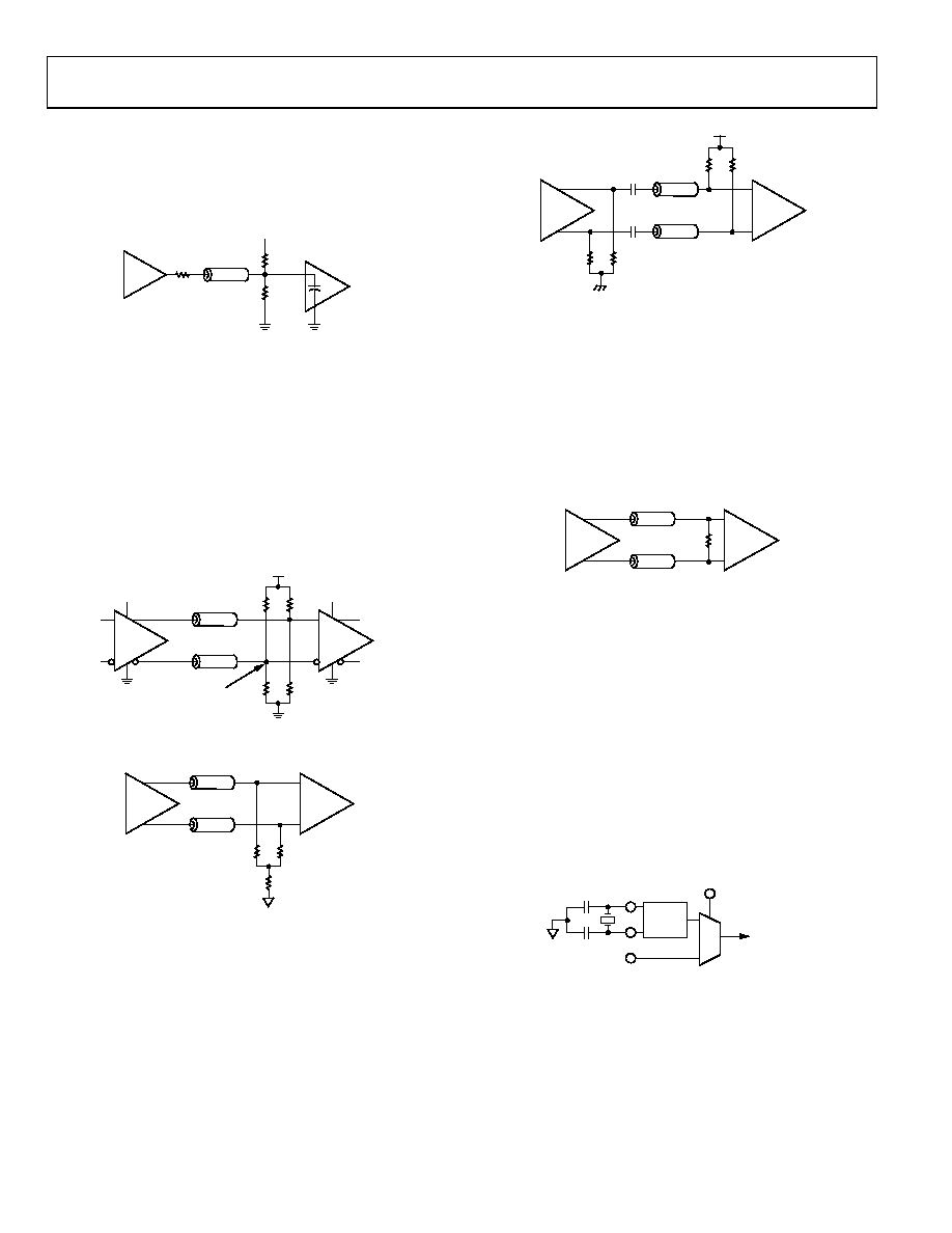
Figure 21. CMOS Output with Far-End Termination
LVPECL CLOCK DISTRIBUTION
The LVPECL outputs, which are open emitter, require a dc
termination to bias the output transistors. The simplified
equivalent circuit in Figure 19 shows the LVPECL output stage.
In most applications, a standard LVPECL far-end termination is
recommended, as shown in Figure 22. The resistor network is
designed to match the transmission line impedance (50 Ω) and
establish a dc bias of (VCC – 2 V). An alternative dc-coupled
LVPECL termination network with a reduced number of
components is also possible as shown in Figure 23.
50
3.3V
SINGLE-ENDED
(NOT COUPLED)
3.3V
LVPECL
127
83
07
49
8-
0
29
VT = VCC – 2.0V
VCC = 3.3V
LVPECL
Figure 22. LVPECL Far-End Termination
50
LVPECL
50
07
498
-03
0
LVPECL
Figure 23. LVPECL Y Termination
An ac- coupled LVPECL termination scheme is shown in
50
LVPECL
50
200
07
49
8-
03
1
LVPECL
VTERM
0.1F
Figure 24. LVPECL AC- Coupled Termination
LVDS CLOCK DISTRIBUTION
The AD9572 is also available with low voltage differential
signaling (LVDS) outputs. LVDS uses a current mode output
stage with a factory programmed current level. The normal
value (default) for this current is 3.5 mA, which yields a 350 mV
output swing across a 100 Ω resistor. The LVDS outputs meet or
exceed all ANSI/TIA/EIA-644 specifications.
A recommended termination circuit for the LVDS outputs is
shown in Figure 25.
50
LVDS
100
07
498
-03
2
LVDS
Figure 25. LVDS Output Termination
See the AN-586 Application Note on the Analog Devices
website at www.analog.com for more information about LVDS.
REFERENCE INPUT
By default, the crystal oscillator is enabled and used as the
reference source, which requires the connection of an external
25 MHz crystal cut to resonate in fundamental mode. The total
load capacitance presented to the oscillator should sum to 14 pF.
In the example shown in Figure 26, parasitic trace capacitance
of 1.5 pF, and an AD9572 input pin capacitance of 1.5 pF are
assumed, with the series combination of the two 22 pF
capacitances providing a further 11 pF. The REFSEL pin is
pulled high internally by about 30 kΩ to support default
operation.
07
498
-03
3
XTAL
OSC
TO PLLs
REFCLK
REFSEL
22pF
Figure 26. Reference Input section
When REFSEL is tied low, the crystal oscillator is powered down,
and the REFCLK pin must provide a good quality 25 MHz
reference clock instead. This single-ended input can be driven
by either a dc-coupled LVCMOS level signal or an ac-coupled
相关PDF资料 |
PDF描述 |
|---|---|
| AD9573ARUZ-RL7 | IC PCI CLCOK GEN 25MHZ 16TSSOP |
| AD9575ARUZPEC | IC PLL CLOCK GEN 25MHZ 16TSSOP |
| AD9577BCPZ-R7 | IC CLOCK GENERATOR 40LFCSP |
| AD9600ABCPZ-150 | IC ADC 10BIT 150MSPS 64LFCSP |
| AD9608BCPZRL7-125 | IC ADC 10BIT 125MSPS 64LFCSP |
相关代理商/技术参数 |
参数描述 |
|---|---|
| AD9572ACPZLVD-RL | 功能描述:IC PLL CLOCK GEN 25MHZ 40LFCSP RoHS:是 类别:集成电路 (IC) >> 时钟/计时 - 时钟发生器,PLL,频率合成器 系列:- 标准包装:1,000 系列:Precision Edge® 类型:时钟/频率合成器 PLL:无 输入:CML,PECL 输出:CML 电路数:1 比率 - 输入:输出:2:1 差分 - 输入:输出:是/是 频率 - 最大:10.7GHz 除法器/乘法器:无/无 电源电压:2.375 V ~ 3.6 V 工作温度:-40°C ~ 85°C 安装类型:表面贴装 封装/外壳:16-VFQFN 裸露焊盘,16-MLF? 供应商设备封装:16-MLF?(3x3) 包装:带卷 (TR) 其它名称:SY58052UMGTRSY58052UMGTR-ND |
| AD9572ACPZPEC | 功能描述:IC PLL CLOCK GEN 25MHZ 40LFCSP RoHS:是 类别:集成电路 (IC) >> 时钟/计时 - 时钟发生器,PLL,频率合成器 系列:- 标准包装:2,000 系列:- 类型:PLL 频率合成器 PLL:是 输入:晶体 输出:时钟 电路数:1 比率 - 输入:输出:1:1 差分 - 输入:输出:无/无 频率 - 最大:1GHz 除法器/乘法器:是/无 电源电压:4.5 V ~ 5.5 V 工作温度:-20°C ~ 85°C 安装类型:表面贴装 封装/外壳:16-LSSOP(0.175",4.40mm 宽) 供应商设备封装:16-SSOP 包装:带卷 (TR) 其它名称:NJW1504V-TE1-NDNJW1504V-TE1TR |
| AD9572ACPZPEC-R7 | 功能描述:IC PLL CLOCK GEN 25MHZ 40LFCSP RoHS:是 类别:集成电路 (IC) >> 时钟/计时 - 时钟发生器,PLL,频率合成器 系列:- 标准包装:1,000 系列:Precision Edge® 类型:时钟/频率合成器 PLL:无 输入:CML,PECL 输出:CML 电路数:1 比率 - 输入:输出:2:1 差分 - 输入:输出:是/是 频率 - 最大:10.7GHz 除法器/乘法器:无/无 电源电压:2.375 V ~ 3.6 V 工作温度:-40°C ~ 85°C 安装类型:表面贴装 封装/外壳:16-VFQFN 裸露焊盘,16-MLF? 供应商设备封装:16-MLF?(3x3) 包装:带卷 (TR) 其它名称:SY58052UMGTRSY58052UMGTR-ND |
| AD9572ACPZPEC-RL | 功能描述:IC PLL CLOCK GEN 25MHZ 40LFCSP RoHS:是 类别:集成电路 (IC) >> 时钟/计时 - 时钟发生器,PLL,频率合成器 系列:- 标准包装:1,000 系列:Precision Edge® 类型:时钟/频率合成器 PLL:无 输入:CML,PECL 输出:CML 电路数:1 比率 - 输入:输出:2:1 差分 - 输入:输出:是/是 频率 - 最大:10.7GHz 除法器/乘法器:无/无 电源电压:2.375 V ~ 3.6 V 工作温度:-40°C ~ 85°C 安装类型:表面贴装 封装/外壳:16-VFQFN 裸露焊盘,16-MLF? 供应商设备封装:16-MLF?(3x3) 包装:带卷 (TR) 其它名称:SY58052UMGTRSY58052UMGTR-ND |
| AD9572-EVALZ-LVD | 制造商:AD 制造商全称:Analog Devices 功能描述:Fiber Channel/Ethernet Clock Generator IC, PLL Core, Dividers, 7 Clock Outputs |
发布紧急采购,3分钟左右您将得到回复。