参数资料
| 型号: | AD9632ANZ |
| 厂商: | Analog Devices Inc |
| 文件页数: | 8/20页 |
| 文件大小: | 0K |
| 描述: | IC OPAMP VF ULDIST 70MA 8DIP |
| 标准包装: | 50 |
| 放大器类型: | 电压反馈 |
| 电路数: | 1 |
| 转换速率: | 1500 V/µs |
| -3db带宽: | 250MHz |
| 电流 - 输入偏压: | 2µA |
| 电压 - 输入偏移: | 2000µV |
| 电流 - 电源: | 16mA |
| 电流 - 输出 / 通道: | 70mA |
| 电压 - 电源,单路/双路(±): | 6 V ~ 12 V,±3 V ~ 6 V |
| 工作温度: | -40°C ~ 85°C |
| 安装类型: | 通孔 |
| 封装/外壳: | 8-DIP(0.300",7.62mm) |
| 供应商设备封装: | 8-PDIP |
| 包装: | 管件 |
AD9631/AD9632
Data Sheet
Rev. D | Page 16 of 20
PULSE RESPONSE
Unlike a traditional voltage feedback amplifier, where the slew
speed is dictated by its front end dc quiescent current and gain
current that increases proportionally to the input step signal
amplitude. This results in slew rates (1300 V/s) comparable
to wideband current feedback designs. This, combined with
relatively low input noise current (2.0 pA/√Hz), gives the
current feedback amplifiers.
LARGE SIGNAL PERFORMANCE
The outstanding large signal operation of the AD9631 and
AD9632 is due to a unique, proprietary design architecture. To
maintain this level of performance, the maximum 550 V × MHz
product must be observed (for example, @ 100 MHz, VOUT ≤
5.5 V p-p).
POWER SUPPLY BYPASSING
Adequate power supply bypassing can be critical when optimiz-
ing the performance of a high frequency circuit. Inductance in
the power supply leads can form resonant circuits that produce
peaking in the amplifier’s response. In addition, if large current
transients must be delivered to the load, then bypass capacitors
(typically greater than 1 F) will be required to provide the best
settling time and lowest distortion. A parallel combination of at
least 4.7 F, and between 0.1 F and 0.01 F, is recommended.
Some brands of electrolytic capacitors will require a small series
damping resistor ≈4.7 for optimum results.
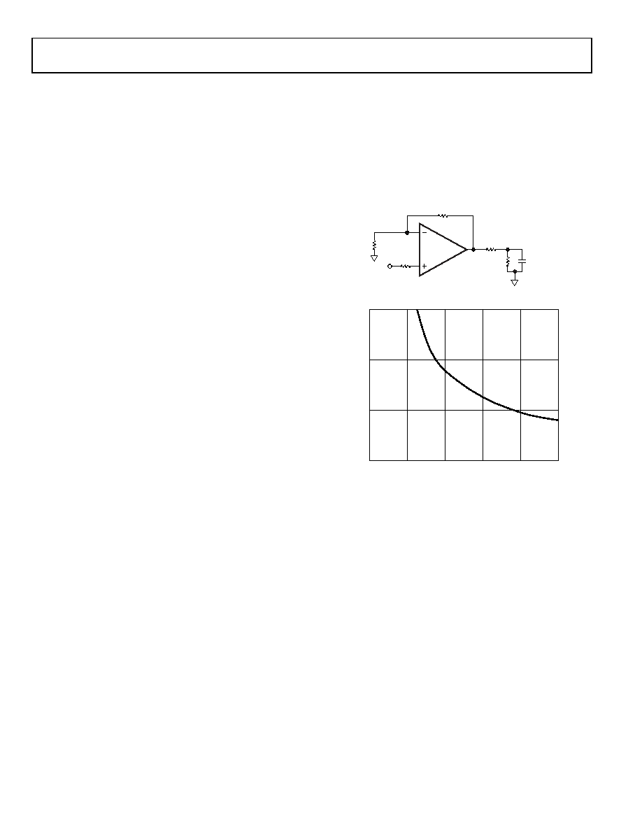
DRIVING CAPACITIVE LOADS
reactive loads. If driving loads with a capacitive component is
desired, the best frequency response is obtained by the addition
of a small series resistance as shown in Figure 62. Figure 63
shows the optimum value for RSERIES vs. capacitive load. It is
worth noting that the frequency response of the circuit when
driving large capacitive loads will be dominated by the passive
roll-off of RSERIES and CL.
Figure 62. Driving Capacitive Loads
Figure 63. Recommended RSERIES vs. Capacitive Load
RF
RSERIES
RIN
CL
RL
1kΩ
AD9631/
AD9632
00601-
062
40
30
20
10
0
10
20
5
15
25
R
SER
IES
(Ω)
CL (pF)
00601-
063
相关PDF资料 |
PDF描述 |
|---|---|
| RNCP0805FTD15K0 | RES 15K OHM 1/4W 1% 0805 SMD |
| AD629BR | IC AMP DIFF 25MA LDRIFT 8SOIC |
| 1-521253-2 | CONN RCPT HSG 2POS .250 RED |
| AD9632AR | IC OPAMP VF ULDIST 70MA 8SOIC |
| LT2179IS#TRPBF | IC OPAMP MICROPOWER QUAD 14SOIC |
相关代理商/技术参数 |
参数描述 |
|---|---|
| AD9632AR | 功能描述:IC OPAMP VF ULDIST 70MA 8SOIC RoHS:否 类别:集成电路 (IC) >> Linear - Amplifiers - Instrumentation 系列:- 标准包装:2,500 系列:Excalibur™ 放大器类型:J-FET 电路数:1 输出类型:- 转换速率:45 V/µs 增益带宽积:10MHz -3db带宽:- 电流 - 输入偏压:20pA 电压 - 输入偏移:490µV 电流 - 电源:1.7mA 电流 - 输出 / 通道:48mA 电压 - 电源,单路/双路(±):4.5 V ~ 38 V,±2.25 V ~ 19 V 工作温度:-40°C ~ 85°C 安装类型:表面贴装 封装/外壳:8-SOIC(0.154",3.90mm 宽) 供应商设备封装:8-SOIC 包装:带卷 (TR) |
| AD9632AR-EBZ | 功能描述:BOARD EVAL FOR AD9632AR RoHS:是 类别:编程器,开发系统 >> 评估板 - 运算放大器 系列:- 产品培训模块:Lead (SnPb) Finish for COTS Obsolescence Mitigation Program 标准包装:1 系列:- |
| AD9632AR-REEL | 制造商:Analog Devices 功能描述:OP Amp Single Volt Fdbk ±6V 8-Pin SOIC N T/R 制造商:Rochester Electronics LLC 功能描述:WIDE BW, GAIN=2 OP AMP - Tape and Reel |
| AD9632AR-REEL7 | 制造商:Analog Devices 功能描述:OP Amp Single Volt Fdbk 制造商:Analog Devices 功能描述:IC OP-AMP HIGH SPEED |
| AD9632ARZ | 功能描述:IC OPAMP VF ULDIST 70MA 8SOIC RoHS:是 类别:集成电路 (IC) >> Linear - Amplifiers - Instrumentation 系列:- 标准包装:2,500 系列:- 放大器类型:通用 电路数:4 输出类型:- 转换速率:0.6 V/µs 增益带宽积:1MHz -3db带宽:- 电流 - 输入偏压:45nA 电压 - 输入偏移:2000µV 电流 - 电源:1.4mA 电流 - 输出 / 通道:40mA 电压 - 电源,单路/双路(±):3 V ~ 32 V,±1.5 V ~ 16 V 工作温度:0°C ~ 70°C 安装类型:表面贴装 封装/外壳:14-TSSOP(0.173",4.40mm 宽) 供应商设备封装:14-TSSOP 包装:带卷 (TR) 其它名称:LM324ADTBR2G-NDLM324ADTBR2GOSTR |
发布紧急采购,3分钟左右您将得到回复。