- 您现在的位置:买卖IC网 > PDF目录1988 > AD9637BCPZRL7-80 (Analog Devices Inc)IC ADC 12BIT SRL 80MSPS 64LFCSP PDF资料下载
参数资料
| 型号: | AD9637BCPZRL7-80 |
| 厂商: | Analog Devices Inc |
| 文件页数: | 15/40页 |
| 文件大小: | 0K |
| 描述: | IC ADC 12BIT SRL 80MSPS 64LFCSP |
| 标准包装: | 750 |
| 位数: | 12 |
| 采样率(每秒): | 80M |
| 数据接口: | LVDS,串行,SPI? |
| 转换器数目: | 8 |
| 功率耗散(最大): | 574mW |
| 电压电源: | 模拟和数字 |
| 工作温度: | -40°C ~ 85°C |
| 安装类型: | 表面贴装 |
| 封装/外壳: | 64-VFQFN 裸露焊盘,CSP |
| 供应商设备封装: | 64-LFCSP-VQ(9x9) |
| 包装: | * |
| 输入数目和类型: | 8 个差分 |
第1页第2页第3页第4页第5页第6页第7页第8页第9页第10页第11页第12页第13页第14页当前第15页第16页第17页第18页第19页第20页第21页第22页第23页第24页第25页第26页第27页第28页第29页第30页第31页第32页第33页第34页第35页第36页第37页第38页第39页第40页
AD9637
Data Sheet
Rev. A | Page 22 of 40
Jitter Considerations
High speed, high resolution ADCs are sensitive to the quality of the
clock input. The degradation in SNR at a given input frequency
(fA) due only to aperture jitter (tJ) can be calculated by
SNR Degradation = 20 log10
×
J
A
t
f
π
2
1
In this equation, the rms aperture jitter represents the root mean
square of all jitter sources, including the clock input, analog input
signal, and ADC aperture jitter specifications. IF undersampling
applications are particularly sensitive to jitter (see Figure 55).
The clock input should be treated as an analog signal in cases
where aperture jitter may affect the dynamic range of the AD9637.
Power supplies for clock drivers should be separated from the
ADC output driver supplies to avoid modulating the clock signal
with digital noise. Low jitter, crystal-controlled oscillators make
the best clock sources. If the clock is generated from another
type of source (by gating, dividing, or other methods), it should
be retimed by the original clock at the last step.
Refer to the AN-501 Application Note and the AN-756
Application Note for more in-depth information about jitter
performance as it relates to ADCs.
1
10
100
1000
16 BITS
14 BITS
12 BITS
30
40
50
60
70
80
90
100
110
120
130
0.125ps
0.25ps
0.5ps
1.0ps
2.0ps
ANALOG INPUT FREQUENCY (MHz)
10 BITS
8 BITS
RMS CLOCK JITTER REQUIREMENT
S
NR
(
d
B)
10215-
054
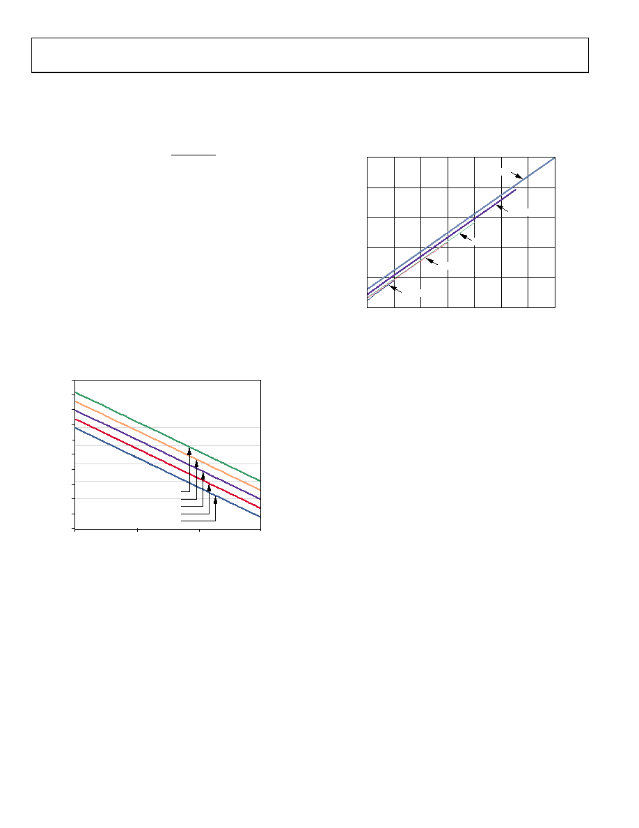
Figure 55. Ideal SNR vs. Input Frequency and Jitter
POWER DISSIPATION AND POWER-DOWN MODE
As shown in Figure 56, the power dissipated by the AD9637 is
proportional to its sample rate. The digital power dissipation
does not vary significantly because it is determined primarily by
the DRVDD supply and bias current of the LVDS output drivers.
10215-
055
400
300
350
250
200
150
10
ANAL
O
G
P
O
W
E
R
(
mW
)
SAMPLE RATE (MSPS)
20
30
40
50
60
70
80
65MSPS
80MSPS
50MSPS
40MSPS
20MSPS
Figure 56. Analog Core Power vs. fSAMPLE for fIN = 9.7 MHz
The AD9637 is placed in power-down mode either by the SPI
port or by asserting the PDWN pin high. In this state, the ADC
typically dissipates 1 mW. During power-down, the output drivers
are placed in a high impedance state. Asserting the PDWN pin
low returns the AD9637 to its normal operating mode. Note
that PDWN is referenced to the digital output driver supply
(DRVDD) and should not exceed that supply voltage.
Low power dissipation in power-down mode is achieved by
shutting down the reference, reference buffer, biasing networks,
and clock. Internal capacitors are discharged when entering
power-down mode and then must be recharged when returning
to normal operation. As a result, wake-up time is related to the
time spent in power-down mode, and shorter power-down
cycles result in proportionally shorter wake-up times. When
using the SPI port interface, the user can place the ADC in
power-down mode or standby mode. Standby mode allows the
user to keep the internal reference circuitry powered when
faster wake-up times are required. See the Memory Map section
for more details on using these features.
相关PDF资料 |
PDF描述 |
|---|---|
| AD9639BCPZ-170 | IC ADC 12B 170MSPS QUAD 72LFCSP |
| AD9640ABCPZ-125 | IC ADC 14BIT 125MSPS 64LFCSP |
| AD9641BCPZ-80 | IC ADC 14BIT SRL 80MSPS 32LFCSP |
| AD9644BCPZ-80 | IC ADC 14BIT 80MSPS 3V 48LFCSP |
| AD9648BCPZRL7-125 | IC ADC 14BIT 125MSPS 64LFCSP |
相关代理商/技术参数 |
参数描述 |
|---|---|
| AD9639-210KITZ | 功能描述:模数转换器 - ADC Quad 12 Bit 210 MSPS Seria 1.8V ADC EB RoHS:否 制造商:Analog Devices 通道数量: 结构: 转换速率: 分辨率: 输入类型: 信噪比: 接口类型: 工作电源电压: 最大工作温度: 安装风格: 封装 / 箱体: |
| AD9639BCPZ-170 | 功能描述:IC ADC 12B 170MSPS QUAD 72LFCSP RoHS:是 类别:集成电路 (IC) >> 数据采集 - 模数转换器 系列:- 产品培训模块:Lead (SnPb) Finish for COTS Obsolescence Mitigation Program 标准包装:250 系列:- 位数:12 采样率(每秒):1.8M 数据接口:并联 转换器数目:1 功率耗散(最大):1.82W 电压电源:模拟和数字 工作温度:-40°C ~ 85°C 安装类型:表面贴装 封装/外壳:48-LQFP 供应商设备封装:48-LQFP(7x7) 包装:管件 输入数目和类型:2 个单端,单极 |
| AD9639BCPZ-210 | 功能描述:IC ADC 12B 170MSPS QUAD 72LFCSP RoHS:是 类别:集成电路 (IC) >> 数据采集 - 模数转换器 系列:- 标准包装:1 系列:microPOWER™ 位数:8 采样率(每秒):1M 数据接口:串行,SPI? 转换器数目:1 功率耗散(最大):- 电压电源:模拟和数字 工作温度:-40°C ~ 125°C 安装类型:表面贴装 封装/外壳:24-VFQFN 裸露焊盘 供应商设备封装:24-VQFN 裸露焊盘(4x4) 包装:Digi-Reel® 输入数目和类型:8 个单端,单极 产品目录页面:892 (CN2011-ZH PDF) 其它名称:296-25851-6 |
| AD9639BCPZRL-170 | 功能描述:IC ADC 12B 170MSPS QUAD 72LFCSP RoHS:是 类别:集成电路 (IC) >> 数据采集 - 模数转换器 系列:- 产品培训模块:Lead (SnPb) Finish for COTS Obsolescence Mitigation Program 标准包装:250 系列:- 位数:12 采样率(每秒):1.8M 数据接口:并联 转换器数目:1 功率耗散(最大):1.82W 电压电源:模拟和数字 工作温度:-40°C ~ 85°C 安装类型:表面贴装 封装/外壳:48-LQFP 供应商设备封装:48-LQFP(7x7) 包装:管件 输入数目和类型:2 个单端,单极 |
| AD9639BCPZRL-210 | 功能描述:模数转换器 - ADC Quad 12 Bit 210 MSPS Seria 1.8V ADC RoHS:否 制造商:Analog Devices 通道数量: 结构: 转换速率: 分辨率: 输入类型: 信噪比: 接口类型: 工作电源电压: 最大工作温度: 安装风格: 封装 / 箱体: |
发布紧急采购,3分钟左右您将得到回复。