- 您现在的位置:买卖IC网 > PDF目录17059 > AD9705-DPG2-EBZ (Analog Devices Inc)BOARD EVAL FOR AD9705 PDF资料下载
参数资料
| 型号: | AD9705-DPG2-EBZ |
| 厂商: | Analog Devices Inc |
| 文件页数: | 32/44页 |
| 文件大小: | 0K |
| 描述: | BOARD EVAL FOR AD9705 |
| 标准包装: | 1 |
| 系列: | * |
第1页第2页第3页第4页第5页第6页第7页第8页第9页第10页第11页第12页第13页第14页第15页第16页第17页第18页第19页第20页第21页第22页第23页第24页第25页第26页第27页第28页第29页第30页第31页当前第32页第33页第34页第35页第36页第37页第38页第39页第40页第41页第42页第43页第44页

AD9704/AD9705/AD9706/AD9707
Data Sheet
Rev. B | Page 38 of 44
0
20
30
507090
10
40
60
80
I CL
K
V
DD
(m
A
)
fCLOCK (MSPS)
05
92
6-
0
99
0.2
0.6
0.4
0.8
1.0
1.2
1.4
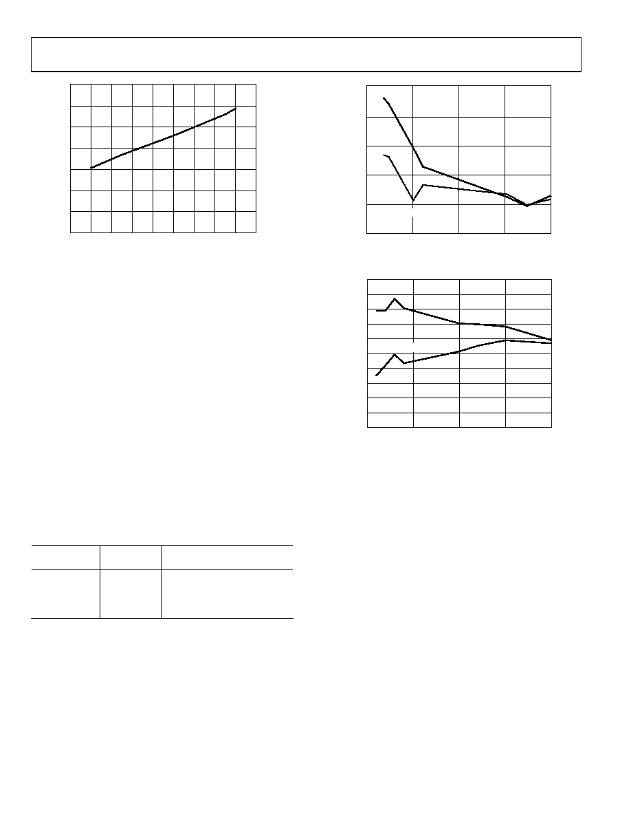
Figure 85. ICLKVDD vs. fCLOCK (Differential Clock Mode) at CLKVDD = 1.8 V
Sleep Operation (Pin Mode)
turns off the output current and reduces the total power consumed
by the device. This mode is activated by applying a Logic 1 to
the SLEEP/CSB pin. The SLEEP/CSB pin logic threshold is
equal to 0.5 × DVDD. This digital input also contains an active
pull-down circuit.
power down and approximately 5 μs to power back up, when
3.3 V AVDD is used.
Sleep and Power-Down Operation (SPI Mode)
functions that can be controlled through the SPI. These power-
down modes can be used to minimize the power dissipation of
the device. The power-down functions are controlled through
Register 0x00, Bit 1 to Bit 3, of the SPI registers. Table 25
summarizes the power-down functions that can be controlled
through the SPI. The power-down mode can be enabled by
writing a Logic 1 to the corresponding bit in Register 0x00.
Table 25. Power-Down Mode Selection
Power-Down
Mode
(Reg. 0x00)
Bit Number
Functional Description
Clock Off
1
Turn off clock
Sleep
2
Turn off output current
Power Down
3
Turn off output current and
internal band gap reference
SELF-CALIBRATION
feature that improves the DNL of the device. Performing a self-
calibration on the device improves device performance in low
frequency applications. The device performance in applications
where the analog output frequencies are above 1 MHz are generally
influenced more by dynamic device behavior than by DNL, and
in these cases, self-calibration is unlikely to provide any benefits
self-calibration is helpful up to 20 MHz for two-tone IMD spaced
10 kHz apart.
88
86
84
82
80
78
0
0.2
0.4
0.6
0.8
059
26
-09
6
S
F
DR
(
d
B
c)
fOUT (MHz)
CALIBRATED
UNCALIBRATED
Figure 86. AD9707 SFDR vs. fOUT at 175 MSPS and IOUTFS = 2 mA
88
87
86
85
84
83
82
81
80
78
79
0
5
10
15
20
05
92
6-
0
97
IM
D
(
d
Bc
)
LOWER
fOUT (MHz)
CALIBRATED
UNCALIBRATED
Figure 87. IMD vs. Lower fOUT at 175 MSPS and IOUTFS = 2 mA
The calibration clock frequency is equal to the DAC clock divided
by the division factor chosen by the DIVSEL value. The frequency
of the calibration clock must be set to under 10 MHz for reliable
calibrations. Best results are obtained by setting DIVSEL[2:0]
(Register 0x0E, Bit 2 to Bit 0) to produce the lowest frequency
calibration clock frequency that the system requirements of the
user allows.
To perform a device self-calibration, use the following procedure:
1
Enable the calibration clock by setting the CALCLK
bit (Register 0x02, Bit 0).
2
Enable self-calibration by writing 0x40 to Register
0x0F.
3
Wait approximately 4500 calibration clock cycles. Each
calibration clock cycle is between 2 DAC clock cycles
and 256 DAC clock cycles, depending on the value of
DIVSEL[2:0].
4
Check if the self-calibration has completed by reading
the CALSTAT bit (Register 0x0F, Bit 7). A Logic 1
indicates the calibration has completed.
5
When the self-calibration has completed, write 0x00
to Register 0x0F.
6
Disable the calibration clock by clearing the CALCLK
bit (Register 0x02, Bit 0).
相关PDF资料 |
PDF描述 |
|---|---|
| MIC2026-2YM | IC DISTRIBUTION SW DUAL 8-SOIC |
| UVZ2E331MRD | CAP ALUM 330UF 250V 20% RADIAL |
| VE-B5B-EY | CONVERTER MOD DC/DC 95V 50W |
| AD9783-DPG2-EBZ | BOARD EVAL FOR AD9783 |
| AD9707-DPG2-EBZ | BOARD EVAL FOR AD9707 |
相关代理商/技术参数 |
参数描述 |
|---|---|
| AD9705EB | 制造商:Rochester Electronics LLC 功能描述: 制造商:Analog Devices 功能描述: |
| AD9705-EB | 制造商:AD 制造商全称:Analog Devices 功能描述:8-/10-/12-/14-Bit, 175 MSPS TxDAC D/A Converters |
| AD9705-EBZ | 功能描述:BOARD EVAL FOR AD9705 RoHS:是 类别:编程器,开发系统 >> 评估板 - 数模转换器 (DAC) 系列:TxDAC® 产品培训模块:Lead (SnPb) Finish for COTS Obsolescence Mitigation Program 标准包装:1 系列:- DAC 的数量:4 位数:12 采样率(每秒):- 数据接口:串行,SPI? 设置时间:3µs DAC 型:电流/电压 工作温度:-40°C ~ 85°C 已供物品:板 已用 IC / 零件:MAX5581 |
| AD9706BCPZ | 功能描述:IC DAC TX 12BIT 175MSPS 32-LFCSP RoHS:是 类别:集成电路 (IC) >> 数据采集 - 数模转换器 系列:TxDAC® 产品培训模块:Lead (SnPb) Finish for COTS Obsolescence Mitigation Program 标准包装:50 系列:- 设置时间:4µs 位数:12 数据接口:串行 转换器数目:2 电压电源:单电源 功率耗散(最大):- 工作温度:-40°C ~ 85°C 安装类型:表面贴装 封装/外壳:8-TSSOP,8-MSOP(0.118",3.00mm 宽) 供应商设备封装:8-uMAX 包装:管件 输出数目和类型:2 电压,单极 采样率(每秒):* 产品目录页面:1398 (CN2011-ZH PDF) |
| AD9706BCPZRL7 | 功能描述:IC DAC TX 12BIT 175MSPS 32-LFCSP RoHS:是 类别:集成电路 (IC) >> 数据采集 - 数模转换器 系列:TxDAC® 标准包装:47 系列:- 设置时间:2µs 位数:14 数据接口:并联 转换器数目:1 电压电源:单电源 功率耗散(最大):55µW 工作温度:-40°C ~ 85°C 安装类型:表面贴装 封装/外壳:28-SSOP(0.209",5.30mm 宽) 供应商设备封装:28-SSOP 包装:管件 输出数目和类型:1 电流,单极;1 电流,双极 采样率(每秒):* |
发布紧急采购,3分钟左右您将得到回复。