- 您现在的位置:买卖IC网 > PDF目录17059 > AD9707-DPG2-EBZ (Analog Devices Inc)BOARD EVAL FOR AD9707 PDF资料下载
参数资料
| 型号: | AD9707-DPG2-EBZ |
| 厂商: | Analog Devices Inc |
| 文件页数: | 7/44页 |
| 文件大小: | 0K |
| 描述: | BOARD EVAL FOR AD9707 |
| 标准包装: | 1 |
| 系列: | * |
第1页第2页第3页第4页第5页第6页当前第7页第8页第9页第10页第11页第12页第13页第14页第15页第16页第17页第18页第19页第20页第21页第22页第23页第24页第25页第26页第27页第28页第29页第30页第31页第32页第33页第34页第35页第36页第37页第38页第39页第40页第41页第42页第43页第44页
Data Sheet
AD9704/AD9705/AD9706/AD9707
Rev. B | Page 15 of 44
AD9704
TOP VIEW
(Not to Scale)
PIN 1
INDICATOR
8
7
6
5
4
3
2
1
NC
DVDD
DB0 (LSB)
DB1
17
18
19
20
21
22
23
24
PIN/SPI/RESET
AVDD
OTCM
IOUTB
IOUTA
ACOM
REFIO
FS ADJ
16
15
14
13
12
11
10
9
M
O
DE
/S
DI
O
CM
O
DE
/S
CL
K
CL
KV
DD
CL
KCO
M
CL
K–
CL
K
+
DCO
M
NC
25
26
27
28
29
30
31
32
SL
EEP
/C
SB
DCO
M
DB7
(
M
S
B
)
DB6
DB5
DB4
DB3
DB2
05
92
6-
0
84
NOTES
1. NC = NO CONNECT. DO NOT CONNECT TO THIS PIN.
2. IT IS RECOMMENDED THAT THE EXPOSED PAD BE
THERMALLY CONNECTED TO A COPPER GROUND
PLANE FOR ENHANCED ELECTRICAL AND THERMAL
PERFORMANCE.
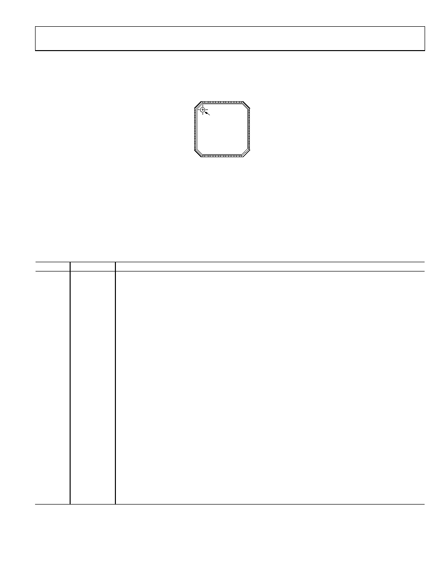
Figure 6. AD9704 Pin Configuration
Table 12. AD9704 Pin Function Descriptions
Pin No.
Mnemonic
Description
28 to 32, 1
DB6 to DB1
Data Bit 6 to Data Bit 1.
2
DB0 (LSB)
Least Significant Data Bit (LSB).
3
DVDD
Digital Supply Voltage (1.7 V to 3.6 V).
4 to 9
NC
No Connect.
10, 26
DCOM
Digital Common.
11
CLKVDD
Clock Supply Voltage (1.7 V to 3.6 V).
12
CLK+
Positive Differential Clock Input.
13
CLK
Negative Differential Clock Input.
14
CLKCOM
Clock Common.
15
CMODE/SCLK
In pin mode, this pin selects the clock input type. Connect to CLKCOM for single-ended clock receiver (drive CLK+
and float CLK). Connect to CLKVDD for differential receiver. In SPI mode, this pin is the serial data clock input.
16
MODE/SDIO
In pin mode, this pin selects the input data format. Connect to DCOM for straight binary, and DVDD for twos
complement. In SPI mode, this pin acts as SPI data input/output.
17
PIN/SPI/RESET
Selects SPI Mode or Pin Mode Operation. Active high for pin mode operation and active low for SPI mode
operation. Pulse high to reset SPI registers to default values.
18
AVDD
Analog Supply Voltage (1.7 V to 3.6 V).
19
OTCM
Adjustable Output Common Mode. Refer to the Theory of Operation section for details.
20
IOUTB
Complementary DAC Current Output. Full-scale current is sourced when all data bits are 0s.
21
IOUTA
DAC Current Output. Full-scale current is sourced when all data bits are 1s.
22
ACOM
Analog Common.
23
REFIO
Reference Input/Output. Serves as reference input when internal reference disabled. Serves as 1.0 V reference output
when internal reference is activated. Requires a 0.1 μF capacitor to ACOM when internal reference is activated.
24
FS ADJ
Full-Scale Current Output Adjust.
25
SLEEP/CSB
In pin mode, active high powers down chip. In SPI mode, this pin is the serial port chip select (active low).
27
DB7 (MSB)
Most Significant Data Bit (MSB).
EPAD
It is recommended that the exposed pad be thermally connected to a copper ground plane for enhanced
electrical and thermal performance.
相关PDF资料 |
PDF描述 |
|---|---|
| AD9704-DPG2-EBZ | BOARD EVAL FOR AD9704 |
| AD9741-DPG2-EBZ | IC DAC DUAL 8BIT 200MSPS 72LFCSP |
| 0210490186 | CABLE JUMPER 1.25MM .254M 12POS |
| AD9743-DPG2-EBZ | IC DAC DUAL 10BIT 72LFCSP |
| AD9116-DPG2-EBZ | IC DAC DUAL 12BIT LO PWR 40LFCSP |
相关代理商/技术参数 |
参数描述 |
|---|---|
| AD9707-EB | 制造商:AD 制造商全称:Analog Devices 功能描述:8-/10-/12-/14-Bit, 175 MSPS TxDAC D/A Converters |
| AD9707-EBZ | 制造商:Analog Devices 功能描述:Evaluation Board For AD9707 DigitalToAnalog Converters 8/10/12/14Bit, 175 MSPS TxDAC |
| AD9708 | 制造商:AD 制造商全称:Analog Devices 功能描述:8-Bit, 100 MSPS TxDAC D/A Converter |
| AD9708AR | 功能描述:IC DAC 8BIT 100MSPS 28-SOIC RoHS:否 类别:集成电路 (IC) >> 数据采集 - 数模转换器 系列:TxDAC® 标准包装:47 系列:- 设置时间:2µs 位数:14 数据接口:并联 转换器数目:1 电压电源:单电源 功率耗散(最大):55µW 工作温度:-40°C ~ 85°C 安装类型:表面贴装 封装/外壳:28-SSOP(0.209",5.30mm 宽) 供应商设备封装:28-SSOP 包装:管件 输出数目和类型:1 电流,单极;1 电流,双极 采样率(每秒):* |
发布紧急采购,3分钟左右您将得到回复。