参数资料
| 型号: | AD9708AR |
| 厂商: | Analog Devices Inc |
| 文件页数: | 12/16页 |
| 文件大小: | 0K |
| 描述: | IC DAC 8BIT 100MSPS 28-SOIC |
| 产品培训模块: | Data Converter Fundamentals DAC Architectures |
| 标准包装: | 27 |
| 系列: | TxDAC® |
| 设置时间: | 35ns |
| 位数: | 8 |
| 数据接口: | 并联 |
| 转换器数目: | 1 |
| 电压电源: | 模拟和数字 |
| 功率耗散(最大): | 175mW |
| 工作温度: | -40°C ~ 85°C |
| 安装类型: | 表面贴装 |
| 封装/外壳: | 28-SOIC(0.295",7.50mm 宽) |
| 供应商设备封装: | 28-SOIC W |
| 包装: | 管件 |
| 输出数目和类型: | 2 电流,单极;2 电流,双极 |
| 采样率(每秒): | 125M |
| 配用: | AD9708-EBZ-ND - BOARD EVAL FOR AD9708 |
AD9708
–5–
REV. B
DEFINITIONS OF SPECIFICATIONS
Linearity Error (Also Called Integral Nonlinearity or INL)
Linearity error is defined as the maximum deviation of the
actual analog output from the ideal output, determined by a
straight line drawn from zero to full scale.
Differential Nonlinearity (or DNL)
DNL is the measure of the variation in analog value, normalized
to full scale, associated with a 1 LSB change in digital input code.
Monotonicity
A D/A converter is monotonic if the output either increases or
remains constant as the digital input increases.
Offset Error
The deviation of the output current from the ideal of zero is
called offset error. For IOUTA, 0 mA output is expected when
the inputs are all 0s. For IOUTB, 0 mA output is expected
when all inputs are set to 1s.
Gain Error
The difference between the actual and ideal output span. The
actual span is determined by the output when all inputs are set
to 1s minus the output when all inputs are set to 0s.
Output Compliance Range
The range of allowable voltage at the output of a current-output
DAC. Operation beyond the maximum compliance limits may
cause either output stage saturation or breakdown resulting in
nonlinear performance.
Temperature Drift
Temperature drift is specified as the maximum change from the
ambient (+25
°C) value to the value at either T
MIN or TMAX. For
offset and gain drift, the drift is reported in ppm of full-scale
range (FSR) per degree C. For reference drift, the drift is
reported in ppm per degree C.
Power Supply Rejection
The maximum change in the full-scale output as the supplies
are varied from nominal to minimum and maximum specified
voltages.
Settling Time
The time required for the output to reach and remain within a
specified error band about its final value, measured from the
start of the output transition.
Glitch Impulse
Asymmetrical switching times in a DAC give rise to undesired
output transients that are quantified by a glitch impulse. It is
specified as the net area of the glitch in pV-s.
Spurious-Free Dynamic Range
The difference, in dB, between the rms amplitude of the output
signal and the peak spurious signal over the specified bandwidth.
Signal-to-Noise and Distortion (S/N+D, SINAD) Ratio
S/N+D is the ratio of the rms value of the measured output
signal to the rms sum of all other spectral components below the
Nyquist frequency, including harmonics but excluding dc. The
value for S/N+D is expressed in decibels.
Total Harmonic Distortion
THD is the ratio of the rms sum of the first six harmonic
components to the rms value of the measured output signal. It is
expressed as a percentage or in decibels (dB).
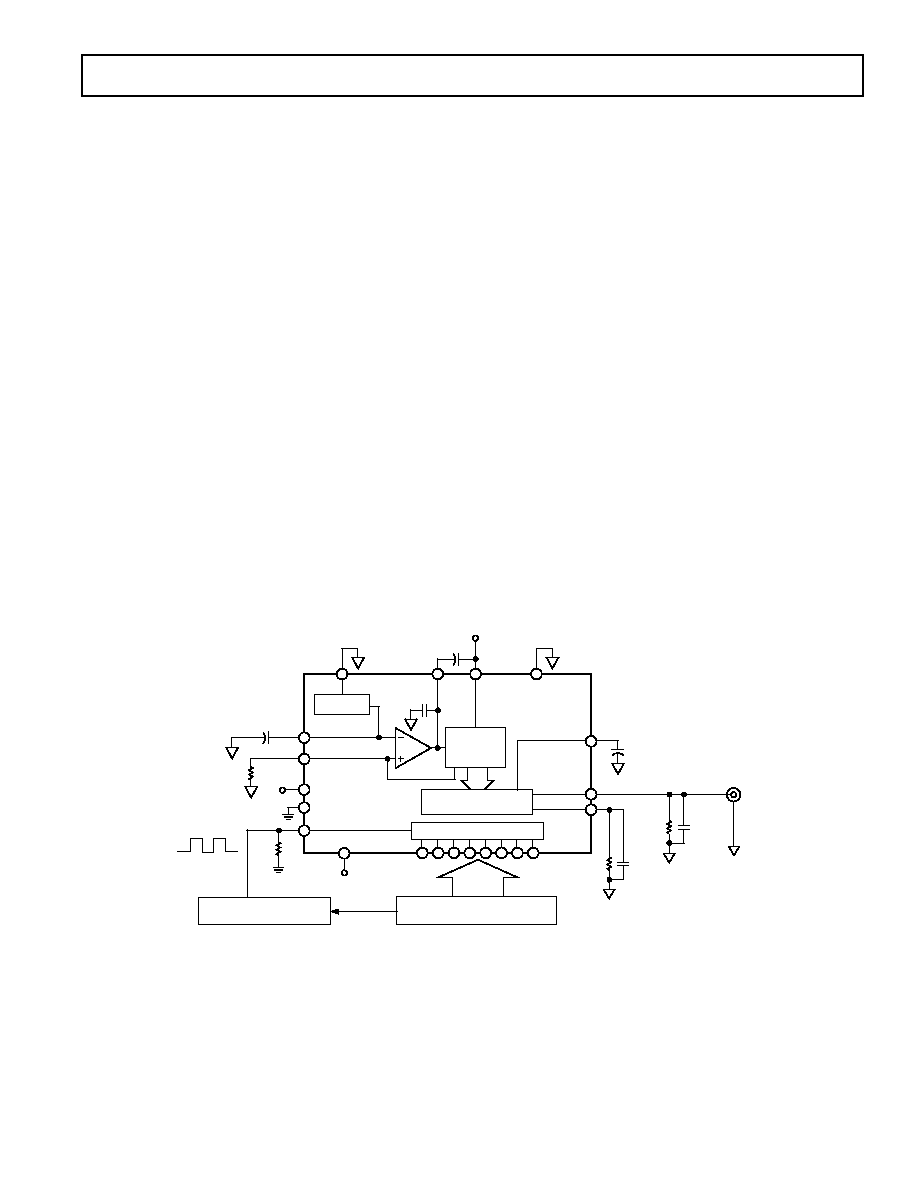
DVDD
DCOM
RETIMED
CLOCK
OUTPUT*
DIGITAL
DATA
TEKTRONIX
AWG-2021
LECROY 9210
PULSE GENERATOR
CLOCK
OUTPUT
50
20pF
50
20pF
TO HP3589A
SPECTRUM/
NETWORK
ANALYZER
50
INPUT
* AWG2021 CLOCK RETIMED
SUCH THAT DIGITAL DATA
TRANSITIONS ON FALLING EDGE
OF 50% DUTY CYCLE CLOCK.
+1.20V REF
REFLO
REF IO
FS ADJ
50pF
COMP1
0.1 F
CURRENT
SOURCE
ARRAY
+5V
AVDD
SEGMENTED
SWITCHES
LATCHES
DVDD
DCOM
CLOCK
SLEEP
IOUTA
IOUTB
COMP2
ACOM
0.1 F
+5V
RSET
2k
0.1 F
AD9708
50
Figure 2. Basic AC Characterization Test Setup
相关PDF资料 |
PDF描述 |
|---|---|
| AD8300ARZ-REEL | IC DAC 12BIT SERIAL 8SOIC |
| VI-J0J-MY | CONVERTER MOD DC/DC 36V 50W |
| VE-J1Y-MY | CONVERTER MOD DC/DC 3.3V 33W |
| VE-23Z-MU-B1 | CONVERTER MOD DC/DC 2V 80W |
| VE-J1Y-MX | CONVERTER MOD DC/DC 3.3V 49.5W |
相关代理商/技术参数 |
参数描述 |
|---|---|
| AD9708ARRL | 制造商:Analog Devices 功能描述:DAC 1-CH Segment 8-bit 28-Pin SOIC W T/R 制造商:Rochester Electronics LLC 功能描述:8 BIT 125 MSPS+ TXDAC D/A CONVERTER - Tape and Reel |
| AD9708ARU | 功能描述:IC DAC 8BIT 100MSPS 28-TSSOP RoHS:否 类别:集成电路 (IC) >> 数据采集 - 数模转换器 系列:TxDAC® 标准包装:47 系列:- 设置时间:2µs 位数:14 数据接口:并联 转换器数目:1 电压电源:单电源 功率耗散(最大):55µW 工作温度:-40°C ~ 85°C 安装类型:表面贴装 封装/外壳:28-SSOP(0.209",5.30mm 宽) 供应商设备封装:28-SSOP 包装:管件 输出数目和类型:1 电流,单极;1 电流,双极 采样率(每秒):* |
| AD9708ARURL | 功能描述:INTEGRATED CIRCUIT 制造商:analog devices inc. 系列:* 包装:带卷(TR) 零件状态:最後搶購 封装/外壳:28-TSSOP(0.173",4.40mm 宽) 供应商器件封装:28-TSSOP 标准包装:1 |
| AD9708ARURL7 | 功能描述:IC DAC 8BIT 100MSPS 28-TSSOP RoHS:否 类别:集成电路 (IC) >> 数据采集 - 数模转换器 系列:TxDAC® 产品培训模块:LTC263x 12-, 10-, and 8-Bit VOUT DAC Family 特色产品:LTC2636 - Octal 12-/10-/8-Bit SPI VOUT DACs with 10ppm/°C Reference 标准包装:91 系列:- 设置时间:4µs 位数:10 数据接口:MICROWIRE?,串行,SPI? 转换器数目:8 电压电源:单电源 功率耗散(最大):2.7mW 工作温度:-40°C ~ 85°C 安装类型:表面贴装 封装/外壳:14-WFDFN 裸露焊盘 供应商设备封装:14-DFN-EP(4x3) 包装:管件 输出数目和类型:8 电压,单极 采样率(每秒):* |
| AD9708ARUZ | 功能描述:IC DAC 8BIT 100MSPS 28-TSSOP RoHS:是 类别:集成电路 (IC) >> 数据采集 - 数模转换器 系列:TxDAC® 产品培训模块:Lead (SnPb) Finish for COTS Obsolescence Mitigation Program 标准包装:50 系列:- 设置时间:4µs 位数:12 数据接口:串行 转换器数目:2 电压电源:单电源 功率耗散(最大):- 工作温度:-40°C ~ 85°C 安装类型:表面贴装 封装/外壳:8-TSSOP,8-MSOP(0.118",3.00mm 宽) 供应商设备封装:8-uMAX 包装:管件 输出数目和类型:2 电压,单极 采样率(每秒):* 产品目录页面:1398 (CN2011-ZH PDF) |
发布紧急采购,3分钟左右您将得到回复。