- 您现在的位置:买卖IC网 > PDF目录17063 > AD9709-EBZ (Analog Devices Inc)BOARD EVAL FOR AD9709 PDF资料下载
参数资料
| 型号: | AD9709-EBZ |
| 厂商: | Analog Devices Inc |
| 文件页数: | 9/32页 |
| 文件大小: | 0K |
| 描述: | BOARD EVAL FOR AD9709 |
| 产品培训模块: | DAC Architectures |
| 标准包装: | 1 |
| 系列: | TxDAC® |
| DAC 的数量: | 2 |
| 位数: | 8 |
| 采样率(每秒): | 125M |
| 数据接口: | 并联 |
| 设置时间: | 35ns |
| DAC 型: | 电流 |
| 工作温度: | -40°C ~ 85°C |
| 已供物品: | 板 |
| 已用 IC / 零件: | AD9709 |
| 相关产品: | AD9709ASTZRL-ND - IC DAC 8BIT DUAL 125MSPS 48LQFP AD9709ASTZ-ND - IC DAC 8BIT DUAL 125MSPS 48-LQFP |
第1页第2页第3页第4页第5页第6页第7页第8页当前第9页第10页第11页第12页第13页第14页第15页第16页第17页第18页第19页第20页第21页第22页第23页第24页第25页第26页第27页第28页第29页第30页第31页第32页
AD9709
Rev. B | Page 17 of 32
Digital signal paths should be kept short, and run lengths should be
matched to avoid propagation delay mismatch. The insertion of
a low value (that is, 20 Ω to 100 Ω) resistor network between
the AD9709 digital inputs and driver outputs may be helpful in
reducing any overshooting and ringing at the digital inputs that
contribute to digital feedthrough. For longer board traces and
high data update rates, stripline techniques with proper
impedance and termination resistors should be considered to
maintain “clean” digital inputs.
The external clock driver circuitry provides the AD9709 with a
low-jitter clock input meeting the minimum and maximum logic
levels while providing fast edges. Fast clock edges help minimize
jitter manifesting itself as phase noise on a reconstructed waveform.
Therefore, the clock input should be driven by the fastest logic
family suitable for the application.
Note that the clock input can also be driven via a sine wave, which
is centered around the digital threshold (that is, DVDDx/2) and
meets the minimum and maximum logic threshold. This typically
results in a slight degradation in the phase noise, which becomes
more noticeable at higher sampling rates and output frequencies.
In addition, at higher sampling rates, the 20% tolerance of the
digital logic threshold should be considered because it affects
the effective clock duty cycle and, subsequently, cut into the
required data setup and hold times.
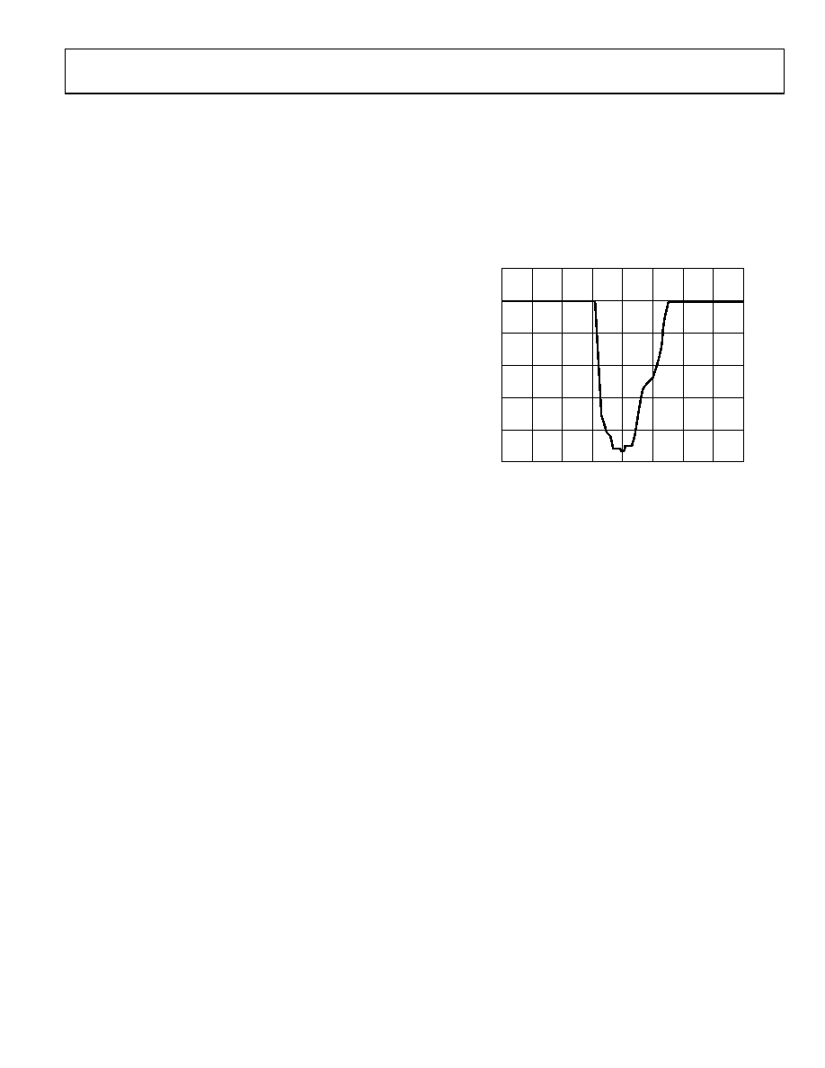
Input Clock and Data Timing Relationship
SNR in a DAC is dependent on the relationship between the
position of the clock edges and the point in time at which the
input data changes. The AD9709 is rising-edge triggered and
therefore exhibits SNR sensitivity when the data transition is
close to this edge. In general, the goal when applying the AD9709 is
to make the data transition close to the falling clock edge. This
becomes more important as the sample rate increases. Figure 32
shows the relationship of SNR to clock/data placement.
60
50
40
30
20
10
0
–4
–3
–2
–1
0
1
2
3
4
S
NR
(
d
Bc)
TIME OF DATA CHANGE RELATIVE TO
RISING CLOCK EDGE (ns)
00
60
6-
03
1
Figure 32. SNR vs. Clock Placement @ fOUT = 20 MHz and fCLK = 125 MSPS
相关PDF资料 |
PDF描述 |
|---|---|
| RBM11DRTI-S13 | CONN EDGECARD 22POS .156 EXTEND |
| ECM25DCSN | CONN EDGECARD 50POS DIP .156 SLD |
| AD9708-EBZ | BOARD EVAL FOR AD9708 |
| RBM11DRKI-S13 | CONN EDGECARD 22POS .156 EXTEND |
| AD9706-EBZ | BOARD EVAL FOR AD9706 |
相关代理商/技术参数 |
参数描述 |
|---|---|
| AD9709-EBZ1 | 制造商:AD 制造商全称:Analog Devices 功能描述:8-Bit, 125 MSPS, Dual TxDAC Digital-to-Analog Converter |
| AD9712 | 制造商:AD 制造商全称:Analog Devices 功能描述:12-BIT, 100MSPS D/A CONVERTERS |
| ad97128bsq/883b | 制造商:Analog Devices 功能描述: |
| AD9712AJN | 制造商:未知厂家 制造商全称:未知厂家 功能描述:12-Bit Digital-to-Analog Converter |
| AD9712AJP | 制造商:未知厂家 制造商全称:未知厂家 功能描述:12-Bit Digital-to-Analog Converter |
发布紧急采购,3分钟左右您将得到回复。