- 您现在的位置:买卖IC网 > PDF目录8647 > AD9715BCPZRL7 (Analog Devices Inc)IC DAC DUAL 10BIT LO PWR 40LFCSP PDF资料下载
参数资料
| 型号: | AD9715BCPZRL7 |
| 厂商: | Analog Devices Inc |
| 文件页数: | 26/80页 |
| 文件大小: | 0K |
| 描述: | IC DAC DUAL 10BIT LO PWR 40LFCSP |
| 产品培训模块: | Data Converter Fundamentals DAC Architectures |
| 标准包装: | 750 |
| 系列: | TxDAC® |
| 位数: | 10 |
| 数据接口: | 串行 |
| 转换器数目: | 2 |
| 电压电源: | 模拟和数字 |
| 功率耗散(最大): | 86mW |
| 工作温度: | -40°C ~ 85°C |
| 安装类型: | 表面贴装 |
| 封装/外壳: | 40-VFQFN 裸露焊盘,CSP |
| 供应商设备封装: | 40-LFCSP-VQ(6x6) |
| 包装: | 带卷 (TR) |
| 输出数目和类型: | 4 电流,单极 |
| 采样率(每秒): | 125M |
第1页第2页第3页第4页第5页第6页第7页第8页第9页第10页第11页第12页第13页第14页第15页第16页第17页第18页第19页第20页第21页第22页第23页第24页第25页当前第26页第27页第28页第29页第30页第31页第32页第33页第34页第35页第36页第37页第38页第39页第40页第41页第42页第43页第44页第45页第46页第47页第48页第49页第50页第51页第52页第53页第54页第55页第56页第57页第58页第59页第60页第61页第62页第63页第64页第65页第66页第67页第68页第69页第70页第71页第72页第73页第74页第75页第76页第77页第78页第79页第80页
AD9714/AD9715/AD9716/AD9717
Rev. A | Page 32 of 80
THEORY OF OPERATION
I DAC
Q DAC
AUX1DAC
AUX2DAC
BAND
GAP
CLOCK
DIST
10k
QRSET
16k
IRSET
16k
IREF
100A
IRCML
1k TO
250
QRCML
1k TO
250
500
SPI
INTERFACE
1 INTO 2
INTERLEAVED
DATA
INTERFACE
I DATA
Q DATA
1.8V
LDO
1V
AD9717
07
26
5-
0
46
RLIN
IOUTN
IOUTP
RLIP
AVDD
AVSS
RLQP
QOUTP
QOUTN
RLQN
DB11
DB10
DB9
DB8
DVDDIO
DVSS
DVDD
DB7
DB6
DB5
DB
12
DB
13
(
M
S
B
)
SD
IO
/F
O
R
M
A
T
S
C
LK
/C
LK
M
D
R
ESE
T
/PI
N
M
D
RE
F
IO
F
S
AD
JI
/AUX
I
FS
A
D
JQ
/A
U
X
Q
CM
L
I
DB4
DB3
DB2
DB1
DB
0(
L
S
B
)
DC
L
K
IO
CV
D
CL
KI
N
C
VSS
CM
L
Q
C
S
/P
W
R
D
N
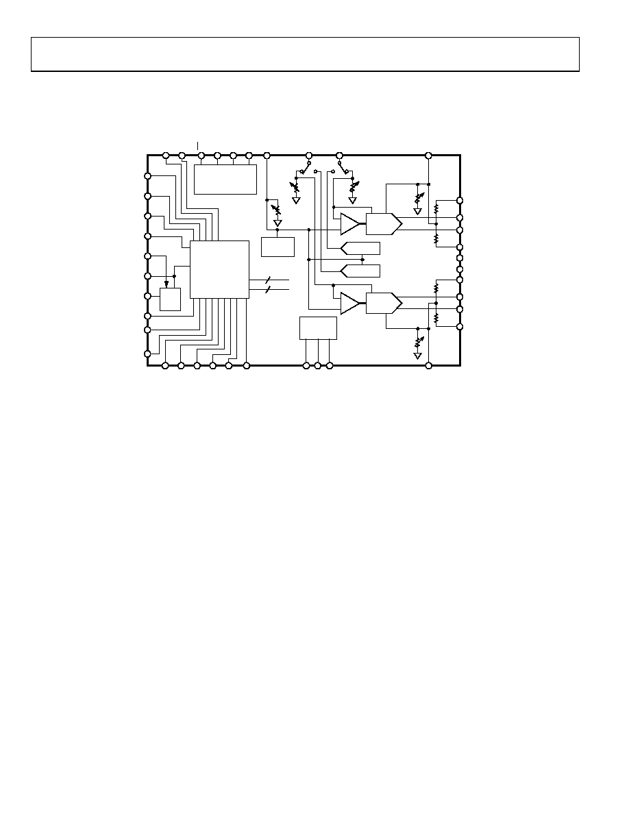
Figure 84. Simplified Block Diagram
Figure 84 shows a simplified block diagram of the AD9714/
AD9715/AD9716/AD9717 that consists of two DACs, digital
control logic, and a full-scale output current control. Each DAC
contains a PMOS current source array capable of providing a
nominal full-scale current (IxOUTFS) of 2 mA and a maximum of
4 mA. The arrays are divided into 31 equal currents that make
up the five most significant bits (MSBs). The next four bits, or
middle bits, consist of 15 equal current sources whose value is
1/16 of an MSB current source. The remaining LSBs are binary
weighted fractions of the current sources of the middle bits.
Implementing the middle and lower bits with current sources,
instead of an R-2R ladder, enhances its dynamic performance
for multitone or low amplitude signals and helps maintain the
high output impedance of the DACs (that is, >200 MΩ).
All of these current sources are switched to one or the other
of the two output nodes (IOUTP or IOUTN) via PMOS differential
current switches. The switches are based on the architecture that
was pioneered in the AD976x family, with further refinements
to reduce distortion contributed by the switching transient. This
switch architecture also reduces various timing errors and
provides matching complementary drive signals to the inputs
of the differential current switches.
The analog and digital I/O sections of the AD9714/AD9715/
AD9716/AD9717 have separate power supply inputs (AVDD and
DVDDIO) that can operate independently over a 1.8 V to 3.3 V
range. The core digital section requires 1.8 V. An optional on-chip
LDO is provided for DVDDIO supplies greater than 1.8 V, or the
1.8 V can be supplied directly through DVDD. A 1.0 μF bypass
capacitor at DVDD (Pin 7) is required when using the LDO.
The core is capable of operating at a rate of up to 125 MSPS. It
consists of edge-triggered latches and the segment decoding logic
circuitry. The analog section includes PMOS current sources,
associated differential switches, a 1.0 V band gap voltage
reference, and a reference control amplifier.
Each DAC full-scale output current is regulated by the reference
control amplifier and can be set from 1 mA to 4 mA via an external
resistor, xRSET, connected to its full-scale adjust pin (FSADJx).
The external resistor, in combination with both the reference
control amplifier and voltage reference, VREFIO, sets the reference
current, IxREF, which is replicated to the segmented current sources
with the proper scaling factor. The full-scale current, IxOUTFS, is
32 × IxREF.
Optional on-chip xRSET resistors are provided that can be pro-
grammed between a nominal value of 8 kΩ to 32 kΩ (4 mA to
1 mA IxOUTFS, respectively).
The AD9714/AD9715/AD9716/AD9717 provide the option of
setting the output common mode to a value other than AVSS
via the output common-mode pins (CMLI and CMLQ). This
facilitates directly interfacing the output of the AD9714/AD9715/
AD9716/AD9717 to components that require common-mode
levels greater than 0 V.
相关PDF资料 |
PDF描述 |
|---|---|
| AD9115BCPZRL7 | IC DAC DUAL 10BIT LO PWR 40LFCSP |
| VE-26F-MW-B1 | CONVERTER MOD DC/DC 72V 100W |
| AD9762ARURL7 | IC DAC 12BIT 100KSPS 28-TSSOP |
| AD9762ARRL | IC DAC 12BIT 100KSPS 28-SOIC |
| AD7545AKRZ-REEL7 | IC DAC 12BIT W/BUFF MULT 20SOIC |
相关代理商/技术参数 |
参数描述 |
|---|---|
| AD9715-DPG2-EBZ | 功能描述:ADC 12BIT DUAL 40LFCSP RoHS:是 类别:编程器,开发系统 >> 评估板 - 数模转换器 (DAC) 系列:TxDAC® 产品培训模块:Lead (SnPb) Finish for COTS Obsolescence Mitigation Program 标准包装:1 系列:- DAC 的数量:4 位数:12 采样率(每秒):- 数据接口:串行,SPI? 设置时间:3µs DAC 型:电流/电压 工作温度:-40°C ~ 85°C 已供物品:板 已用 IC / 零件:MAX5581 |
| AD9715-EBZ | 制造商:Analog Devices 功能描述:DUAL 10 BIT LOW POWER CONVERTER - Boxed Product (Development Kits) |
| AD9716 | 制造商:AD 制造商全称:Analog Devices 功能描述:Dual, 8-/10-/12-/14-Bit Low Power Digital-to-Analog Converters |
| AD9716BCPZ | 功能描述:IC DAC DUAL 12BIT LO PWR 40LFCSP RoHS:是 类别:集成电路 (IC) >> 数据采集 - 数模转换器 系列:TxDAC® 标准包装:1 系列:- 设置时间:4.5µs 位数:12 数据接口:串行,SPI? 转换器数目:1 电压电源:单电源 功率耗散(最大):- 工作温度:-40°C ~ 125°C 安装类型:表面贴装 封装/外壳:8-SOIC(0.154",3.90mm 宽) 供应商设备封装:8-SOICN 包装:剪切带 (CT) 输出数目和类型:1 电压,单极;1 电压,双极 采样率(每秒):* 其它名称:MCP4921T-E/SNCTMCP4921T-E/SNRCTMCP4921T-E/SNRCT-ND |
| AD9716BCPZRL7 | 功能描述:IC DAC DUAL 12BIT LO PWR 40LFCSP RoHS:是 类别:集成电路 (IC) >> 数据采集 - 数模转换器 系列:TxDAC® 标准包装:47 系列:- 设置时间:2µs 位数:14 数据接口:并联 转换器数目:1 电压电源:单电源 功率耗散(最大):55µW 工作温度:-40°C ~ 85°C 安装类型:表面贴装 封装/外壳:28-SSOP(0.209",5.30mm 宽) 供应商设备封装:28-SSOP 包装:管件 输出数目和类型:1 电流,单极;1 电流,双极 采样率(每秒):* |
发布紧急采购,3分钟左右您将得到回复。