- 您现在的位置:买卖IC网 > PDF目录17062 > AD9736-DPG2-EBZ (Analog Devices Inc)BOARD EVAL FOR AD9736 PDF资料下载
参数资料
| 型号: | AD9736-DPG2-EBZ |
| 厂商: | Analog Devices Inc |
| 文件页数: | 39/72页 |
| 文件大小: | 0K |
| 描述: | BOARD EVAL FOR AD9736 |
| 产品培训模块: | DAC Architectures |
| 设计资源: | AD9736-DPG2-EBZ Schematic AD9736-DPG2-EBZ BOM AD9736-DPG2-EBZ Gerber Files |
| 标准包装: | 1 |
| DAC 的数量: | 1 |
| 位数: | 14 |
| 采样率(每秒): | 1.2G |
| 数据接口: | 并联 |
| DAC 型: | 电流 |
| 工作温度: | -40°C ~ 85°C |
| 已供物品: | 板 |
| 已用 IC / 零件: | AD9736 |
第1页第2页第3页第4页第5页第6页第7页第8页第9页第10页第11页第12页第13页第14页第15页第16页第17页第18页第19页第20页第21页第22页第23页第24页第25页第26页第27页第28页第29页第30页第31页第32页第33页第34页第35页第36页第37页第38页当前第39页第40页第41页第42页第43页第44页第45页第46页第47页第48页第49页第50页第51页第52页第53页第54页第55页第56页第57页第58页第59页第60页第61页第62页第63页第64页第65页第66页第67页第68页第69页第70页第71页第72页
AD9734/AD9735/AD9736
Rev. A | Page 44 of 72
DIGITAL BUILT-IN SELF TEST (BIST)
OVERVIEW
The AD973x includes an internal signature generator that
processes incoming data to create unique signatures. These
signatures are read back from the SPI port, allowing verification
of correct data transfer into the AD973x. BIST vectors provided
on the AD973x-EB evaluation board CD check the full width
data input or individual bits for PCB debug, utilizing the
procedure in the AD973X BIST Procedure section. Alterna-
tively, any vector can be used provided the expected signature is
calculated in advance.
The MATLAB routine, in the Generating Expected Signatures
section, calculates the expected signature. BIST verifies correct
data transfer because not all errors are always evident on a
spectrum analyzer. There are four BIST signature generators
that can be read back using Reg. 18 to Reg. 21, based on the
setting of the BIST selection bits (Reg. 17, Bits 7:6), as shown in
Table 24. The BIST signature returned from the AD973x
depends on the digital input during the test. Because the filters
in the DAC have memory, it is important to put the correct idle
value on the DATA input to flush the memory prior to reading
the BIST signature.
Placing the idle value on the data input also allows the BIST to
be set up while the DAC clock is running. The idle value should
be all 0s in unsigned mode (0x0000) and all 0s except for the
MSB in twos complement mode (0x2000).
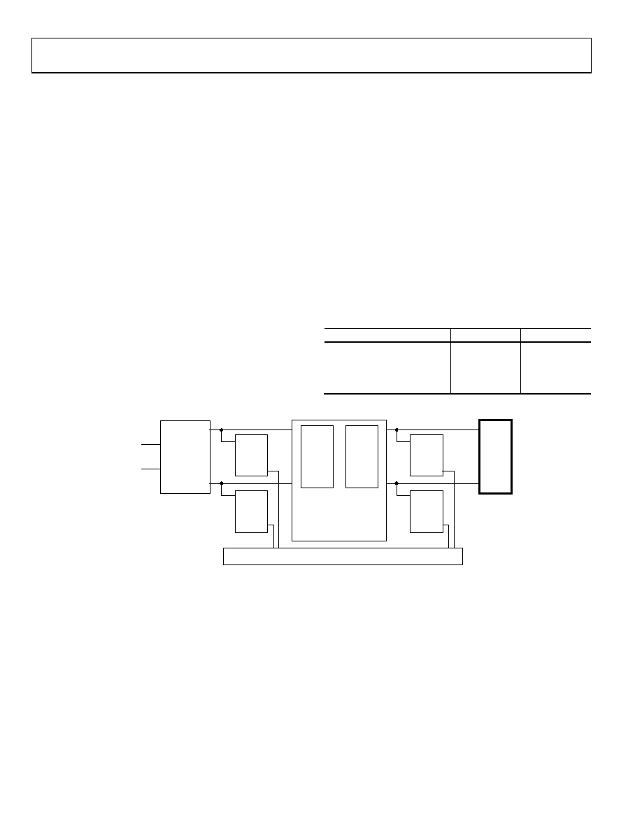
The BIST consists of two stages; the first stage is after the LVDS
receiver and the second stage is after the FIFO. The first BIST
stage verifies correct sampling of the data from the LVDS bus
while the second BIST stage verifies correct synchronization
between the DAC_CLK domain and the DATACLK_IN
domain. The BIST vector is generated using 32-bit LFSR
signature logic. Because the internal architecture is a 2-bus
parallel system, there are two 32-bit LFSR signature logic blocks
on both the LVDS and SYNC blocks. Figure 84 shows where the
LVDS and SYNC phases are located.
Table 24. BIST Selection Bits
Bit
SEL<1>
SEL<0>
LVDS Phase 1
0
LVDS Phase 2
0
1
SYNC Phase 1
1
0
SYNC Phase 2
1
LVDS
RX
DB<13:0>
DATACLK_IN
SYNC LOGIC
FIFO
2x
D1
D2
DAC
LVDS
BIST
PH1
(RISE)
LVDS
BIST
PH2
(FALL)
SYNC
BIST
PH1
(RISE)
SYNC
BIST
PH2
(FALL)
SPI PORT
04862-082
Figure 84. Block Diagram Showing LVDS and SYNC Phase 1 and SYNC Phase 2
相关PDF资料 |
PDF描述 |
|---|---|
| HCM11DSEN-S243 | CONN EDGECARD 22POS .156 EYELET |
| GCB10DHFD | CONN CARDEDGE 20POS .050" SMD |
| AD9786-EBZ | BOARD EVALUATION FOR AD9786 |
| MIC2099-1YMT TR | IC DISTRIBUTION SWITCH |
| RCA10DRMI-S288 | CONN EDGECARD 20POS .125 EXTEND |
相关代理商/技术参数 |
参数描述 |
|---|---|
| AD9736-EB | 制造商:Analog Devices 功能描述:14-BIT, 1.2 GSPS TXDAC+? D/A CONVERTER - Bulk |
| AD9736-EBZ | 制造商:Analog Devices 功能描述:EVAL BD FOR AD9735 DAC, 10-/12-/14BIT, 1200 MSPS DACS - Bulk |
| AD9736XBC | 制造商:Analog Devices 功能描述:14-BIT 1600 MSPS D/A CONVERTER - Bulk |
| AD9737A | 制造商:AD 制造商全称:Analog Devices 功能描述:11-/14-Bit, 2.5 GSPS |
| AD9737ABBCZ | 功能描述:IC DAC 11BIT 2.5GSPS RF 160BGA RoHS:是 类别:集成电路 (IC) >> 数据采集 - 数模转换器 系列:- 标准包装:1 系列:- 设置时间:4.5µs 位数:12 数据接口:串行,SPI? 转换器数目:1 电压电源:单电源 功率耗散(最大):- 工作温度:-40°C ~ 125°C 安装类型:表面贴装 封装/外壳:8-SOIC(0.154",3.90mm 宽) 供应商设备封装:8-SOICN 包装:剪切带 (CT) 输出数目和类型:1 电压,单极;1 电压,双极 采样率(每秒):* 其它名称:MCP4921T-E/SNCTMCP4921T-E/SNRCTMCP4921T-E/SNRCT-ND |
发布紧急采购,3分钟左右您将得到回复。