参数资料
| 型号: | AD9742ARZRL |
| 厂商: | Analog Devices Inc |
| 文件页数: | 9/32页 |
| 文件大小: | 0K |
| 描述: | IC DAC 12BIT 210MSPS 28-SOIC |
| 产品培训模块: | Data Converter Fundamentals DAC Architectures |
| 标准包装: | 1,000 |
| 系列: | TxDAC® |
| 设置时间: | 11ns |
| 位数: | 12 |
| 数据接口: | 并联 |
| 转换器数目: | 1 |
| 电压电源: | 模拟和数字 |
| 功率耗散(最大): | 145mW |
| 工作温度: | -40°C ~ 85°C |
| 安装类型: | 表面贴装 |
| 封装/外壳: | 28-SOIC(0.295",7.50mm 宽) |
| 供应商设备封装: | 28-SOIC W |
| 包装: | 带卷 (TR) |
| 输出数目和类型: | 2 电流,单极;2 电流,双极 |
| 采样率(每秒): | 210M |
| 配用: | AD9742ACP-PCBZ-ND - BOARD EVAL FOR AD9742ACP |
第1页第2页第3页第4页第5页第6页第7页第8页当前第9页第10页第11页第12页第13页第14页第15页第16页第17页第18页第19页第20页第21页第22页第23页第24页第25页第26页第27页第28页第29页第30页第31页第32页
Data Sheet
AD9742
Rev. C | Page 17 of 32
SINGLE-ENDED, UNBUFFERED VOLTAGE OUTPUT
Figure 34 shows the AD9742 configured to provide a unipolar
output range of approximately 0 V to 0.5 V for a doubly terminated
50 cable since the nominal full-scale current, IOUTFS, of 20 mA
flows through the equivalent RLOAD of 25 . In this case, RLOAD
represents the equivalent load resistance seen by IOUTA or
IOUTB. The unused output (IOUTA or IOUTB) can be connected
to ACOM directly or via a matching RLOAD. Different values of
IOUTFS and RLOAD can be selected as long as the positive compliance
range is adhered to. One additional consideration in this mode
is the integral nonlinearity (INL), discussed in the Analog Outputs
section. For optimum INL performance, the single-ended, buffered
voltage output configuration is suggested.
AD9742
IOUTA
IOUTB
50
25
VOUTA = 0V TO 0.5V
IOUTFS = 20mA
50
22
21
02912-B-033
Figure 34. 0 V to 0.5 V Unbuffered Voltage Output
SINGLE-ENDED, BUFFERED VOLTAGE OUTPUT
CONFIGURATION
Figure 35 shows a buffered single-ended output configuration
in which the op amp U1 performs an I-V conversion on the
AD9742 output current. U1 maintains IOUTA (or IOUTB) at a
virtual ground, minimizing the nonlinear output impedance
effect on the DAC’s INL performance as described in the Analog
Outputs section. Although this single-ended configuration typically
provides the best dc linearity performance, its ac distortion
performance at higher DAC update rates may be limited by U1’s
slew rate capabilities. U1 provides a negative unipolar output
voltage, and its full-scale output voltage is simply the product of
RFB and IOUTFS. The full-scale output should be set within U1’s
voltage output swing capabilities by scaling IOUTFS and/or RFB. An
improvement in ac distortion performance may result with a
reduced IOUTFS since U1 will be required to sink less signal current.
AD9742
IOUTA
IOUTB
COPT
200
U1
VOUT = IOUTFS × RFB
IOUTFS = 10mA
RFB
200
22
21
02912-B-034
Figure 35. Unipolar Buffered Voltage Output
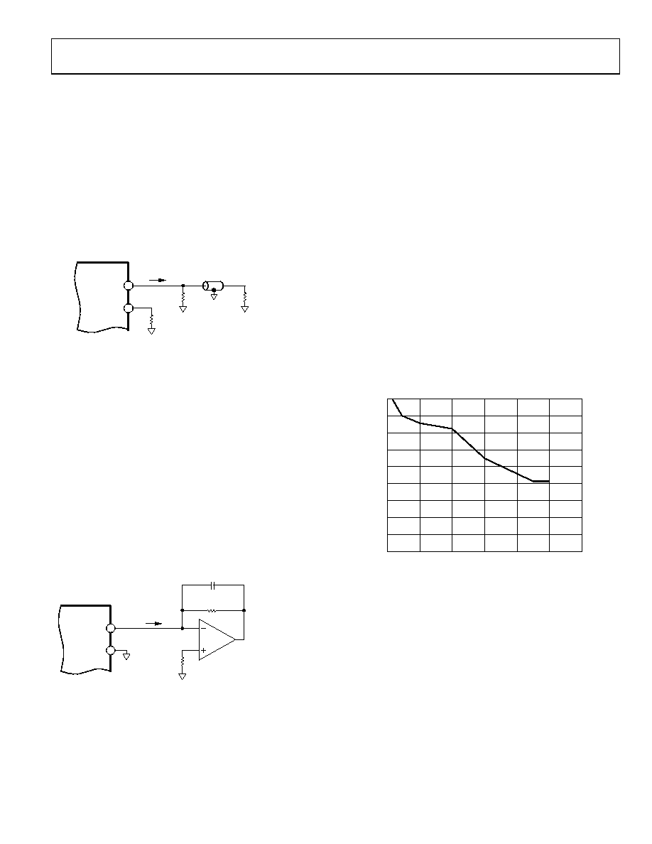
POWER AND GROUNDING CONSIDERATIONS,
POWER SUPPLY REJECTION
Many applications seek high speed and high performance under
less than ideal operating conditions. In these application circuits,
the implementation and construction of the printed circuit
board is as important as the circuit design. Proper RF techniques
must be used for device selection, placement, and routing as
well as power supply bypassing and grounding to ensure
optimum performance. Figure 40 to Figure 43 illustrate the
recommended printed circuit board ground, power, and signal
plane layouts implemented on the AD9742 evaluation board.
One factor that can measurably affect system performance is
the ability of the DAC output to reject dc variations or ac noise
superimposed on the analog or digital dc power distribution.
This is referred to as the power supply rejection ratio (PSRR).
For dc variations of the power supply, the resulting performance
of the DAC directly corresponds to a gain error associated with
the DAC’s full-scale current, IOUTFS. AC noise on the dc supplies
is common in applications where the power distribution is
generated by a switching power supply. Typically, switching
power supply noise will occur over the spectrum from tens of
kHz to several MHz. The PSRR versus frequency of the AD9742
AVDD supply over this frequency range is shown in Figure 36.
FREQUENCY (MHz)
85
40
12
6
8
10
0
PSRR
(dB)
80
75
70
65
60
55
50
2
4
45
02912-B-035
Figure 36. Power Supply Rejection Ratio (PSRR)
Note that the ratio in Figure 36 is calculated as amps out/volts
in. Noise on the analog power supply has the effect of modulating
the internal switches, and therefore the output current. The
voltage noise on AVDD, therefore, will be added in a nonlinear
manner to the desired IOUT. Due to the relative different size of
these switches, the PSRR is very code dependent. This can produce
a mixing effect that can modulate low frequency power supply
noise to higher frequencies. Worst-case PSRR for either one of
the differential DAC outputs will occur when the full-scale current
is directed toward that output. As a result, the PSRR measurement
in Figure 36 represents a worst-case condition in which the
digital inputs remain static and the full-scale output current of
20 mA is directed to the DAC output being measured.
相关PDF资料 |
PDF描述 |
|---|---|
| VI-J1J-MY | CONVERTER MOD DC/DC 36V 50W |
| AD7396ARZ-REEL | IC DAC 12BIT PARALLEL 3V 24-SOIC |
| AD9742ARUZRL7 | IC DAC 12BIT 210MSPS 28-TSSOP |
| VI-B3Z-MU-B1 | CONVERTER MOD DC/DC 2V 80W |
| VI-B3Y-MU-B1 | CONVERTER MOD DC/DC 3.3V 132W |
相关代理商/技术参数 |
参数描述 |
|---|---|
| AD9742-EB | 制造商:Analog Devices 功能描述:EVAL BOARDFOR AD9742 - Bulk |
| AD9742-EBZ | 制造商:AD 制造商全称:Analog Devices 功能描述:12-Bit, 210 MSPS TxDAC Digital-to-Analog Converter |
| AD9743 | 制造商:AD 制造商全称:Analog Devices 功能描述:Dual 8-/10-/12-/14-/16-Bit 250 MSPS Digital-to-Analog Converters |
| AD9743BCPZ | 功能描述:IC DAC 2CH 10BIT 250MSPS 72LFCSP RoHS:是 类别:集成电路 (IC) >> 数据采集 - 数模转换器 系列:- 产品培训模块:Data Converter Fundamentals DAC Architectures 标准包装:750 系列:- 设置时间:7µs 位数:16 数据接口:并联 转换器数目:1 电压电源:双 ± 功率耗散(最大):100mW 工作温度:0°C ~ 70°C 安装类型:表面贴装 封装/外壳:28-LCC(J 形引线) 供应商设备封装:28-PLCC(11.51x11.51) 包装:带卷 (TR) 输出数目和类型:1 电压,单极;1 电压,双极 采样率(每秒):143k |
| AD9743BCPZRL | 功能描述:IC DAC DUAL 10B 250MSPS 72-LFCSP RoHS:是 类别:集成电路 (IC) >> 数据采集 - 数模转换器 系列:- 标准包装:47 系列:- 设置时间:2µs 位数:14 数据接口:并联 转换器数目:1 电压电源:单电源 功率耗散(最大):55µW 工作温度:-40°C ~ 85°C 安装类型:表面贴装 封装/外壳:28-SSOP(0.209",5.30mm 宽) 供应商设备封装:28-SSOP 包装:管件 输出数目和类型:1 电流,单极;1 电流,双极 采样率(每秒):* |
发布紧急采购,3分钟左右您将得到回复。