- 您现在的位置:买卖IC网 > PDF目录17101 > AD9745-DPG2-EBZ (Analog Devices Inc)IC DAC DUAL 12BIT 72LFCSP PDF资料下载
参数资料
| 型号: | AD9745-DPG2-EBZ |
| 厂商: | Analog Devices Inc |
| 文件页数: | 11/28页 |
| 文件大小: | 0K |
| 描述: | IC DAC DUAL 12BIT 72LFCSP |
| 设计资源: | AD9747/6/5/3/1 DPG2 Eval Brd Schematic |
| 标准包装: | 1 |
| DAC 的数量: | 2 |
| 位数: | 12 |
| 采样率(每秒): | 250M |
| 数据接口: | 并联 |
| DAC 型: | 电流 |
| 工作温度: | -40°C ~ 85°C |
| 已供物品: | 板 |
| 已用 IC / 零件: | AD9745 |
第1页第2页第3页第4页第5页第6页第7页第8页第9页第10页当前第11页第12页第13页第14页第15页第16页第17页第18页第19页第20页第21页第22页第23页第24页第25页第26页第27页第28页
Data Sheet
AD9741/AD9743/AD9745/AD9746/AD9747
Rev. A | Page 19 of 28
internally by the serial port controller by decrementing from
the specified address. For LSB-first format, the specified address
is a beginning address or the least significant address in the
current cycle. Remaining register addresses for multiple byte
data transfers are generated internally by the serial port
controller by incrementing from the specified address.
MSB/LSB TRANSFERS
The serial port can support both MSB-first and LSB-first data
formats. This functionality is controlled by Register 0x00, Bit 6.
The default is Logic 0, which is MSB-first format.
When using MSB-first format (LSBFIRST = 0), the instruction
and data bit must be written from MSB to LSB. Multibyte data
transfers in MSB-first format start with an instruction byte that
includes the register address of the most significant data byte.
Subsequent data bytes are loaded into sequentially lower
address locations. In MSB-first mode, the serial port internal
address generator decrements for each byte of the multibyte
data transfer.
When using LSB-first format (LSBFIRST = 1), the instruction
and data bit must be written from LSB to MSB. Multibyte data
transfers in LSB-first format start with an instruction byte that
includes the register address of the least significant data byte.
Subsequent data bytes are loaded into sequentially higher
address locations. In LSB-first mode, the serial port internal
address generator increments for each byte of the multibyte
data transfer.
Use of a single-byte transfer when changing the serial port data
format is recommended to prevent unexpected device behavior.
SERIAL INTERFACE PORT PIN DESCRIPTIONS
Chip Select Bar (CSB)
Active low input starts and gates a communication cycle. It
allows more than one device to be used on the same serial
communication lines. CSB must stay low during the entire
communication cycle. Incomplete data transfers are aborted
anytime the CSB pin goes high. SDO and SDIO pins go to a
high impedance state when this input is high.
Serial Clock (SCLK)
The serial clock pin is used to synchronize data to and from the
device and to run the internal state machines. The maximum
frequency of SCLK is 40 MHz. All data input is registered on
the rising edge of SCLK. All data is driven out on the falling
edge of SCLK.
Serial Data I/O (SDIO)
Data is always written into the device on this pin. However,
SDIO can also function as a bidirectional data output line.
The configuration of this pin is controlled by Register 0x00,
Bit 7. The default is Logic 0, which configures the SDIO pin
as unidirectional.
Serial Data Out (SDO)
Data is read from this pin for protocols that use separate lines
for transmitting and receiving data. The configuration of this
pin is controlled by Register 0x00, Bit 7. If this bit is set to a
Logic 1, the SDO pin does not output data and is set to a high
impedance state.
R/W N1
N0
A4 A3
A2
A1
A0
D7 D6N D5N
D00
D10
D20
D30
D7 D6N D5N
D00
D10
D20
D30
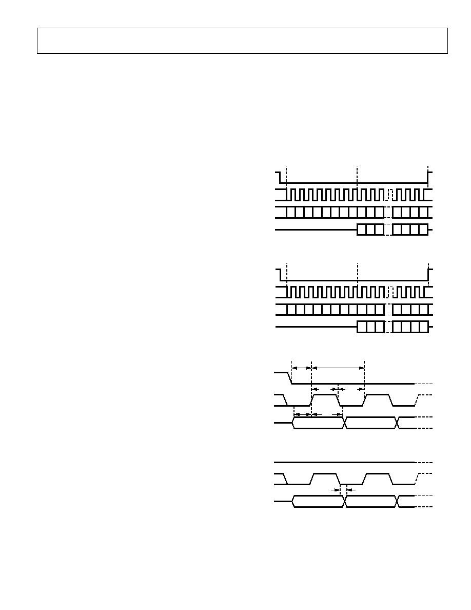
INSTRUCTION CYCLE
DATA TRANSFER CYCLE
CSB
SCLK
SDIO
SDO
06569-
014
Figure 23. Serial Register Interface—MSB First
A0
A1
A2
A3 A4
N0
N1 R/W D00 D10 D20
D7N
D6N
D5N
D4N
D00 D10 D20
D7N
D6N
D5N
D4N
INSTRUCTION CYCLE
DATA TRANSFER CYCLE
CSB
SCLK
SDIO
SDO
06569-
015
Figure 24. Serial Register Interface Timing—LSB First
INSTRUCTION BIT 6
INSTRUCTION BIT 7
CSB
SCLK
SDIO
tS
tDS
tDH
tPWH
tPWL
fSCLK–1
06569-
016
Figure 25. Timing Diagram for SPI Register Write
DATA BIT N – 1
DATA BIT N
CSB
SCLK
SDIO
SDO
tDV
06569-
017
Figure 26. Timing Diagram for SPI Register Read
相关PDF资料 |
PDF描述 |
|---|---|
| RBM25DRXN | CONN EDGECARD 50POS DIP .156 SLD |
| STD24W-Q | WIRE & CABLE MARKERS |
| RBM25DRXH | CONN EDGECARD 50POS DIP .156 SLD |
| 0210490211 | CABLE JUMPER 1.25MM .030M 16POS |
| HL02220GTTR | INDUCTOR 22NH 180MA 0402 |
相关代理商/技术参数 |
参数描述 |
|---|---|
| AD9745-EBZ | 制造商:AD 制造商全称:Analog Devices 功能描述:Dual 8-/10-/12-/14-/16-Bit 250 MSPS Digital-to-Analog Converters |
| AD9746 | 制造商:AD 制造商全称:Analog Devices 功能描述:Dual 8-/10-/12-/14-/16-Bit 250 MSPS Digital-to-Analog Converters |
| AD9746BCPZ | 功能描述:IC DAC DUAL 14B 250MSPS 72LFCSP RoHS:是 类别:集成电路 (IC) >> 数据采集 - 数模转换器 系列:- 产品培训模块:Data Converter Fundamentals DAC Architectures 标准包装:750 系列:- 设置时间:7µs 位数:16 数据接口:并联 转换器数目:1 电压电源:双 ± 功率耗散(最大):100mW 工作温度:0°C ~ 70°C 安装类型:表面贴装 封装/外壳:28-LCC(J 形引线) 供应商设备封装:28-PLCC(11.51x11.51) 包装:带卷 (TR) 输出数目和类型:1 电压,单极;1 电压,双极 采样率(每秒):143k |
| AD9746BCPZRL | 功能描述:IC DAC DUAL 14B 250MSPS 72-LFCSP RoHS:是 类别:集成电路 (IC) >> 数据采集 - 数模转换器 系列:- 产品培训模块:Data Converter Fundamentals DAC Architectures 标准包装:750 系列:- 设置时间:7µs 位数:16 数据接口:并联 转换器数目:1 电压电源:双 ± 功率耗散(最大):100mW 工作温度:0°C ~ 70°C 安装类型:表面贴装 封装/外壳:28-LCC(J 形引线) 供应商设备封装:28-PLCC(11.51x11.51) 包装:带卷 (TR) 输出数目和类型:1 电压,单极;1 电压,双极 采样率(每秒):143k |
| AD9746-DPG2-EBZ | 功能描述:IC DAC DUAL 14BIT 72LFCSP RoHS:是 类别:编程器,开发系统 >> 评估板 - 数模转换器 (DAC) 系列:- 产品培训模块:Lead (SnPb) Finish for COTS Obsolescence Mitigation Program 标准包装:1 系列:- DAC 的数量:4 位数:12 采样率(每秒):- 数据接口:串行,SPI? 设置时间:3µs DAC 型:电流/电压 工作温度:-40°C ~ 85°C 已供物品:板 已用 IC / 零件:MAX5581 |
发布紧急采购,3分钟左右您将得到回复。