参数资料
| 型号: | AD974BNZ |
| 厂商: | Analog Devices Inc |
| 文件页数: | 3/20页 |
| 文件大小: | 0K |
| 描述: | IC DAS 16BIT 4CH 200KSPS 28DIP |
| 标准包装: | 13 |
| 类型: | 数据采集系统(DAS) |
| 分辨率(位): | 16 b |
| 采样率(每秒): | 200k |
| 数据接口: | 串行 |
| 电压电源: | 模拟和数字 |
| 电源电压: | 4.75 V ~ 5.25 V |
| 工作温度: | -40°C ~ 85°C |
| 安装类型: | 通孔 |
| 封装/外壳: | 28-DIP(0.600",15.24mm) |
| 供应商设备封装: | 28-PDIP |
| 包装: | 管件 |
| 配用: | EVAL-AD974CB-ND - BOARD EVAL FOR AD974 |
REV. A
AD974
–11–
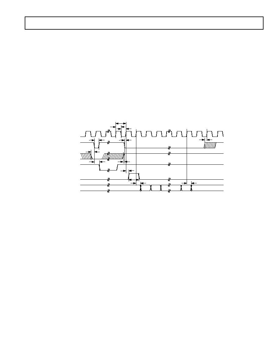
EXTERNAL CONTINUOUS CLOCK DATA READ AFTER
CONVERSION WITH SYNC OUTPUT GENERATED
Figure 8 illustrates the method by which data from conversion
“n” can be read after the conversion is complete using a con-
tinuous external clock, with the generation of a SYNC output.
What permits the generation of a SYNC output is a transition of
DATACLK either while
CS is high or while both CS and R/C are
low.
With a continuous clock the
CS pin cannot be tied low as it
could be with a discontinuous clock. Use of a continuous clock,
while a conversion is occurring, can increase the DNL and
Transition Noise of the AD974.
After a conversion is complete, indicated by
BUSY returning
high, the result of that conversion can be read while
CS is low
and R/
C is high. In Figure 8 clock pulse #0 is used to enable the
generation of a SYNC pulse. The SYNC pulse is actually clocked
out approximately 40 ns after the rising edge of clock pulse #1.
The SYNC pulse will be valid on the falling edge of clock pulse
#1 and the rising edge of clock pulse #2. The MSB will be valid
on the falling edge of clock pulse #2 and the rising edge of clock
pulse #3. The LSB will be valid on the falling edge of clock
pulse #17 and the rising edge of clock pulse #18.
When reading data after the conversion is complete, with the
highest frequency permitted for DATACLK (15.15 MHz) the
maximum possible throughput is approximately 195 kHz and
not the rated 200 kHz.
EXT
DATACLK
CS
R/
C
BUSY
SYNC
DATA
0
t12
t13
t14
1
2
3
4
17
18
t1
t15
t10
t2
t16
t17
t12
t18
t19
BIT 15
(MSB)
BIT 14
BIT 0
(LSB)
Figure 8. Conversion and Read Timing Using an External Continuous Data Clock (EXT/
INT Set to Logic High)
相关PDF资料 |
PDF描述 |
|---|---|
| VI-B53-MY-S | CONVERTER MOD DC/DC 24V 50W |
| AD7891YSZ-1 | IC DAS 12BIT 8CH 44-MQFP |
| MS27497E22A55S | CONN RCPT 55POS WALL MNT W/SCKT |
| VE-B33-IU | CONVERTER MOD DC/DC 24V 200W |
| VI-B4T-MY-S | CONVERTER MOD DC/DC 6.5V 50W |
相关代理商/技术参数 |
参数描述 |
|---|---|
| AD974BR | 功能描述:IC DAS 16BIT 4CH 200KSPS 28-SOIC RoHS:否 类别:集成电路 (IC) >> 数据采集 - ADCs/DAC - 专用型 系列:- 产品培训模块:Lead (SnPb) Finish for COTS Obsolescence Mitigation Program 标准包装:50 系列:- 类型:数据采集系统(DAS) 分辨率(位):16 b 采样率(每秒):21.94k 数据接口:MICROWIRE?,QSPI?,串行,SPI? 电压电源:模拟和数字 电源电压:1.8 V ~ 3.6 V 工作温度:-40°C ~ 85°C 安装类型:表面贴装 封装/外壳:40-WFQFN 裸露焊盘 供应商设备封装:40-TQFN-EP(6x6) 包装:托盘 |
| AD974BRS | 功能描述:IC DAS 16BIT 4CH 200KSPS 28-SSOP RoHS:否 类别:集成电路 (IC) >> 数据采集 - ADCs/DAC - 专用型 系列:- 产品培训模块:Lead (SnPb) Finish for COTS Obsolescence Mitigation Program 标准包装:50 系列:- 类型:数据采集系统(DAS) 分辨率(位):16 b 采样率(每秒):21.94k 数据接口:MICROWIRE?,QSPI?,串行,SPI? 电压电源:模拟和数字 电源电压:1.8 V ~ 3.6 V 工作温度:-40°C ~ 85°C 安装类型:表面贴装 封装/外壳:40-WFQFN 裸露焊盘 供应商设备封装:40-TQFN-EP(6x6) 包装:托盘 |
| AD974BRS-RL7 | 功能描述:IC DAS 16BIT 4CH 200KSPS 28SSOP RoHS:否 类别:集成电路 (IC) >> 数据采集 - ADCs/DAC - 专用型 系列:- 产品培训模块:Lead (SnPb) Finish for COTS Obsolescence Mitigation Program 标准包装:50 系列:- 类型:数据采集系统(DAS) 分辨率(位):16 b 采样率(每秒):21.94k 数据接口:MICROWIRE?,QSPI?,串行,SPI? 电压电源:模拟和数字 电源电压:1.8 V ~ 3.6 V 工作温度:-40°C ~ 85°C 安装类型:表面贴装 封装/外壳:40-WFQFN 裸露焊盘 供应商设备封装:40-TQFN-EP(6x6) 包装:托盘 |
| AD974BRSZ | 功能描述:IC DAS 16BIT 4CH 200KSPS 28-SSOP RoHS:是 类别:集成电路 (IC) >> 数据采集 - ADCs/DAC - 专用型 系列:- 产品培训模块:Lead (SnPb) Finish for COTS Obsolescence Mitigation Program 标准包装:50 系列:- 类型:数据采集系统(DAS) 分辨率(位):16 b 采样率(每秒):21.94k 数据接口:MICROWIRE?,QSPI?,串行,SPI? 电压电源:模拟和数字 电源电压:1.8 V ~ 3.6 V 工作温度:-40°C ~ 85°C 安装类型:表面贴装 封装/外壳:40-WFQFN 裸露焊盘 供应商设备封装:40-TQFN-EP(6x6) 包装:托盘 |
| AD974BRZ | 功能描述:IC DAS 16BIT 4CH 200KSPS 28SOIC RoHS:是 类别:集成电路 (IC) >> 数据采集 - ADCs/DAC - 专用型 系列:- 产品培训模块:Data Converter Basics 标准包装:1 系列:- 类型:电机控制 分辨率(位):12 b 采样率(每秒):1M 数据接口:串行,并联 电压电源:单电源 电源电压:2.7 V ~ 3.6 V,4.5 V ~ 5.5 V 工作温度:-40°C ~ 85°C 安装类型:表面贴装 封装/外壳:100-TQFP 供应商设备封装:100-TQFP(14x14) 包装:剪切带 (CT) 其它名称:296-18373-1 |
发布紧急采购,3分钟左右您将得到回复。