参数资料
| 型号: | AD974BR |
| 厂商: | Analog Devices Inc |
| 文件页数: | 2/20页 |
| 文件大小: | 0K |
| 描述: | IC DAS 16BIT 4CH 200KSPS 28-SOIC |
| 标准包装: | 1 |
| 类型: | 数据采集系统(DAS) |
| 分辨率(位): | 16 b |
| 采样率(每秒): | 200k |
| 数据接口: | 串行 |
| 电压电源: | 模拟和数字 |
| 电源电压: | 4.75 V ~ 5.25 V |
| 工作温度: | -40°C ~ 85°C |
| 安装类型: | 表面贴装 |
| 封装/外壳: | 28-SOIC(0.295",7.50mm 宽) |
| 供应商设备封装: | 28-SOIC W |
| 包装: | 管件 |
| 配用: | EVAL-AD974CB-ND - BOARD EVAL FOR AD974 |
REV. A
AD974
–10–
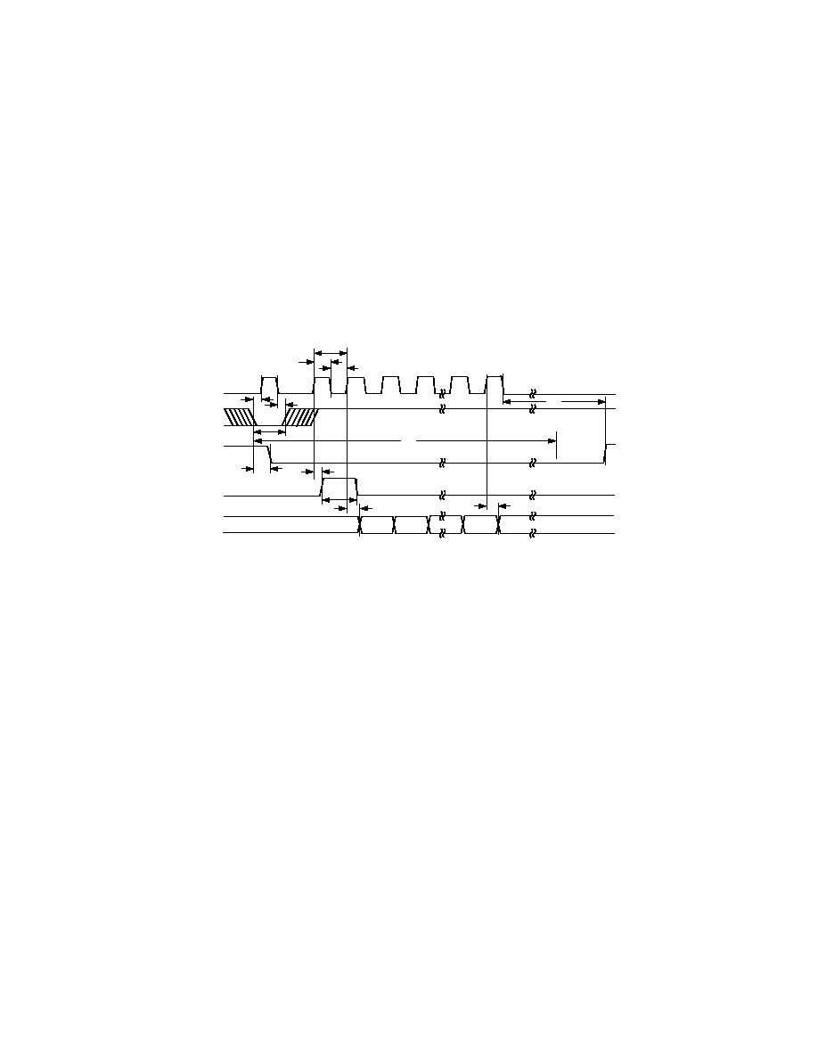
EXTERNAL DISCONTINUOUS CLOCK DATA READ
DURING CONVERSION WITH SYNC OUTPUT
GENERATED
Figure 7 illustrates the method by which data from conversion
“n-1” can be read during conversion “n” while using a discon-
tinuous external clock, with the generation of a SYNC output.
What permits the generation of a SYNC output is a transition of
DATACLK while either
CS is High or while both CS and R/C
are low. In Figure 7 a conversion is initiated by taking R/
C low
with
CS tied low. While this condition exists a transition of
DATACLK, clock pulse #0, will enable the generation of a
SYNC pulse. Less then 83 ns after R/
C is taken low the BUSY
output will go low to indicate that the conversion process has
begun. Figure 7 shows R/
C then going high and after a delay of
greater than 15 ns (t15) clock pulse #1 can be taken high to
request the SYNC output. The SYNC output will appear ap-
proximately 40 ns after this rising edge and will be valid on the
falling edge of clock pulse #1 and the rising edge of clock pulse
#2. The MSB will be valid approximately 40 ns after the rising
edge of clock pulse #2 and can be latched off either the falling
edge of clock pulse #2 or the rising edge of clock pulse #3. The
LSB will be valid on the falling edge of clock pulse #17 and the
rising edge of clock pulse #18.
Data should be clocked out during the first half of
BUSY to
avoid degrading conversion performance. This requires use of a
10 MHz DATACLK or greater, with data being read out as
soon as the conversion process begins.
t12
EXT
DATACLK
R/
C
BUSY
SYNC
DATA
0
t13
t14
t15
t22
t20
t1
t2
t17
t12
t18
BIT 15
(MSB)
BIT 14
BIT 0
(LSB)
1234
17
18
Figure 7. Conversion and Read Timing for Reading Previous Conversion Results During a Conversion
Using External Discontinuous Data Clock (EXT/
INT Set to Logic High, CS Set to Logic Low)
相关PDF资料 |
PDF描述 |
|---|---|
| AD7581BQ | IC ADC DAS 8BIT 8CH 28CDIP |
| AD7891YPZ-1 | IC DAS 12BIT 8CH 44-PLCC |
| LTC6906IS6#TRMPBF | IC OSC SILICON 1MHZ TSOT23-6 |
| AD7891YSZ-2 | IC DAS 12BIT 8CH 44-MQFP |
| LTC6907IS6#TRPBF | IC OSC SILICON 4MHZ TSOT23-6 |
相关代理商/技术参数 |
参数描述 |
|---|---|
| AD974BRS | 功能描述:IC DAS 16BIT 4CH 200KSPS 28-SSOP RoHS:否 类别:集成电路 (IC) >> 数据采集 - ADCs/DAC - 专用型 系列:- 产品培训模块:Lead (SnPb) Finish for COTS Obsolescence Mitigation Program 标准包装:50 系列:- 类型:数据采集系统(DAS) 分辨率(位):16 b 采样率(每秒):21.94k 数据接口:MICROWIRE?,QSPI?,串行,SPI? 电压电源:模拟和数字 电源电压:1.8 V ~ 3.6 V 工作温度:-40°C ~ 85°C 安装类型:表面贴装 封装/外壳:40-WFQFN 裸露焊盘 供应商设备封装:40-TQFN-EP(6x6) 包装:托盘 |
| AD974BRS-RL7 | 功能描述:IC DAS 16BIT 4CH 200KSPS 28SSOP RoHS:否 类别:集成电路 (IC) >> 数据采集 - ADCs/DAC - 专用型 系列:- 产品培训模块:Lead (SnPb) Finish for COTS Obsolescence Mitigation Program 标准包装:50 系列:- 类型:数据采集系统(DAS) 分辨率(位):16 b 采样率(每秒):21.94k 数据接口:MICROWIRE?,QSPI?,串行,SPI? 电压电源:模拟和数字 电源电压:1.8 V ~ 3.6 V 工作温度:-40°C ~ 85°C 安装类型:表面贴装 封装/外壳:40-WFQFN 裸露焊盘 供应商设备封装:40-TQFN-EP(6x6) 包装:托盘 |
| AD974BRSZ | 功能描述:IC DAS 16BIT 4CH 200KSPS 28-SSOP RoHS:是 类别:集成电路 (IC) >> 数据采集 - ADCs/DAC - 专用型 系列:- 产品培训模块:Lead (SnPb) Finish for COTS Obsolescence Mitigation Program 标准包装:50 系列:- 类型:数据采集系统(DAS) 分辨率(位):16 b 采样率(每秒):21.94k 数据接口:MICROWIRE?,QSPI?,串行,SPI? 电压电源:模拟和数字 电源电压:1.8 V ~ 3.6 V 工作温度:-40°C ~ 85°C 安装类型:表面贴装 封装/外壳:40-WFQFN 裸露焊盘 供应商设备封装:40-TQFN-EP(6x6) 包装:托盘 |
| AD974BRZ | 功能描述:IC DAS 16BIT 4CH 200KSPS 28SOIC RoHS:是 类别:集成电路 (IC) >> 数据采集 - ADCs/DAC - 专用型 系列:- 产品培训模块:Data Converter Basics 标准包装:1 系列:- 类型:电机控制 分辨率(位):12 b 采样率(每秒):1M 数据接口:串行,并联 电压电源:单电源 电源电压:2.7 V ~ 3.6 V,4.5 V ~ 5.5 V 工作温度:-40°C ~ 85°C 安装类型:表面贴装 封装/外壳:100-TQFP 供应商设备封装:100-TQFP(14x14) 包装:剪切带 (CT) 其它名称:296-18373-1 |
| AD9750 | 制造商:AD 制造商全称:Analog Devices 功能描述:10-Bit, 125 MSPS High Performance TxDAC D/A Converter |
发布紧急采购,3分钟左右您将得到回复。