参数资料
| 型号: | AD9750ARZRL |
| 厂商: | Analog Devices Inc |
| 文件页数: | 5/22页 |
| 文件大小: | 0K |
| 描述: | IC DAC 10BIT 125MSPS 28SOIC |
| 产品培训模块: | Data Converter Fundamentals DAC Architectures |
| 标准包装: | 1,000 |
| 系列: | TxDAC® |
| 设置时间: | 35ns |
| 位数: | 10 |
| 数据接口: | 并联 |
| 转换器数目: | 1 |
| 电压电源: | 模拟和数字 |
| 功率耗散(最大): | 230mW |
| 工作温度: | -40°C ~ 85°C |
| 安装类型: | 表面贴装 |
| 封装/外壳: | 28-SOIC(0.295",7.50mm 宽) |
| 供应商设备封装: | 28-SOIC W |
| 包装: | 带卷 (TR) |
| 输出数目和类型: | 2 电流,单极;2 电流,双极 |
| 采样率(每秒): | 125M |
| 配用: | AD9750-EB-ND - BOARD EVAL FOR AD9750 |
AD9750
–13–
REV. 0
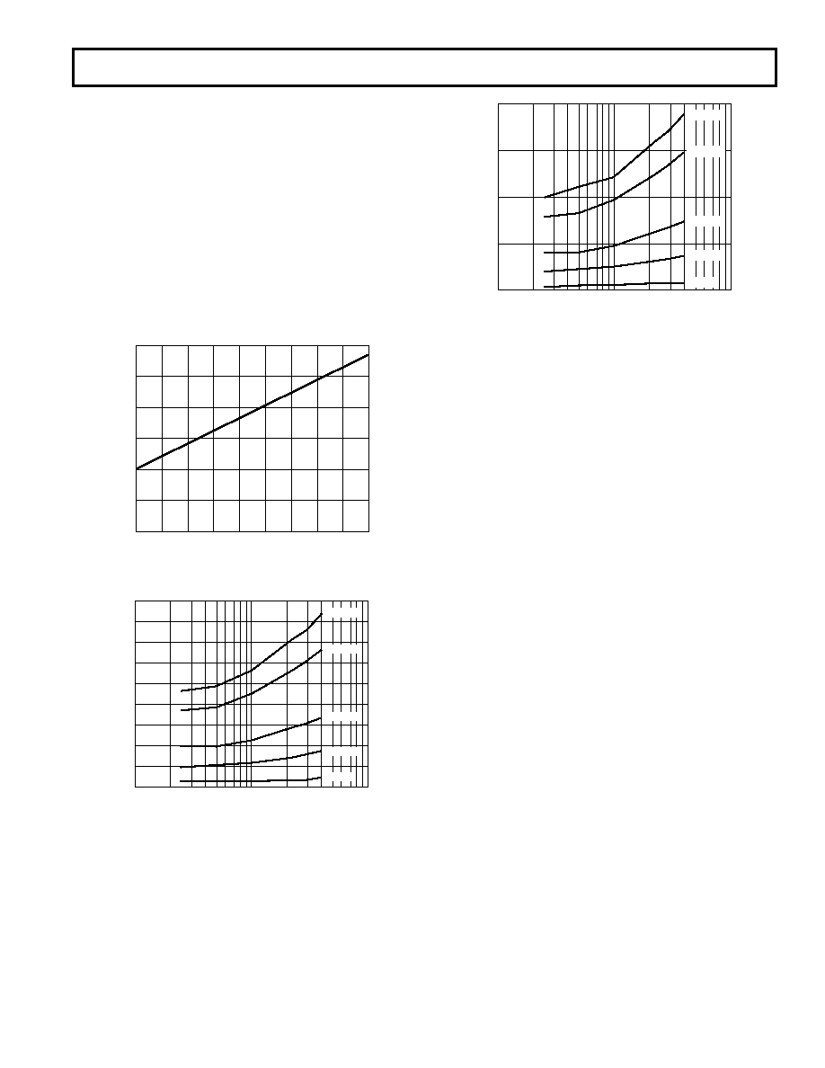
POWER DISSIPATION
The power dissipation, PD, of the AD9750 is dependent on
several factors which include: (1) AVDD and DVDD, the
power supply voltages; (2) IOUTFS, the full-scale current output;
(3) fCLOCK, the update rate; (4) and the reconstructed digital
input waveform. The power dissipation is directly proportional
to the analog supply current, IAVDD, and the digital supply cur-
rent, IDVDD. IAVDD is directly proportional to IOUTFS as shown in
Figure 25 and is insensitive to fCLOCK.
Conversely, IDVDD is dependent on both the digital input wave-
form, fCLOCK, and digital supply DVDD. Figures 26 and 27
show IDVDD as a function of full-scale sine wave output ratios
(fOUT/fCLOCK) for various update rates with DVDD = 5 V and
DVDD = 3 V, respectively. Note, how IDVDD is reduced by more
than a factor of 2 when DVDD is reduced from 5 V to 3 V.
IOUTFS – mA
35
5
220
4
6
8
10
12
141618
30
25
20
15
10
I AVDD
–
mA
Figure 25. IAVDD vs. IOUTFS
RATIO (fCLOCK/fOUT)
18
16
0
0.01
1
0.1
I DVDD
–
mA
8
6
4
2
12
10
14
125MSPS
100MSPS
50MSPS
25MSPS
5MSPS
Figure 26. IDVDD vs. Ratio @ DVDD = 5 V
RATIO (fCLOCK/fOUT)
8
0
0.01
1
0.1
I DVDD
–
mA
6
4
2
125MSPS
100MSPS
50MSPS
25MSPS
5MSPS
Figure 27. IDVDD vs. Ratio @ DVDD = 3 V
APPLYING THE AD9750
OUTPUT CONFIGURATIONS
The following sections illustrate some typical output configura-
tions for the AD9750. Unless otherwise noted, it is assumed
that IOUTFS is set to a nominal 20 mA. For applications requir-
ing the optimum dynamic performance, a differential output
configuration is suggested. A differential output configuration
may consist of either an RF transformer or a differential op amp
configuration. The transformer configuration provides the opti-
mum high frequency performance and is recommended for any
application allowing for ac coupling. The differential op amp
configuration is suitable for applications requiring dc coupling, a
bipolar output, signal gain and/or level shifting.
A single-ended output is suitable for applications requiring a
unipolar voltage output. A positive unipolar output voltage will
result if IOUTA and/or IOUTB is connected to an appropri-
ately sized load resistor, RLOAD, referred to ACOM. This con-
figuration may be more suitable for a single-supply system
requiring a dc coupled, ground referred output voltage. Alterna-
tively, an amplifier could be configured as an I-V converter thus
converting IOUTA or IOUTB into a negative unipolar voltage.
This configuration provides the best dc linearity since IOUTA
or IOUTB is maintained at a virtual ground. Note, IOUTA
provides slightly better performance than IOUTB.
DIFFERENTIAL COUPLING USING A TRANSFORMER
An RF transformer can be used to perform a differential-to-
single-ended signal conversion as shown in Figure 28. A
differentially coupled transformer output provides the optimum
distortion performance for output signals whose spectral content
lies within the transformer’s passband. An RF transformer such
as the Mini-Circuits T1-1T provides excellent rejection of
common-mode distortion (i.e., even-order harmonics) and noise
over a wide frequency range. It also provides electrical isolation
and the ability to deliver twice the power to the load. Trans-
formers with different impedance ratios may also be used for
impedance matching purposes. Note that the transformer
provides ac coupling only.
相关PDF资料 |
PDF描述 |
|---|---|
| V375A36H400BG2 | CONVERTER MOD DC/DC 36V 400W |
| AD7524JR-REEL7 | IC DAC 8BIT MULTIPLYING 16-SOIC |
| V375A28H400BG3 | CONVERTER MOD DC/DC 28V 400W |
| V375A28H400BG | CONVERTER MOD DC/DC 28V 400W |
| AD8802ARU-REEL | IC DAC 8BIT 12CH W/SD 20-TSSOP |
相关代理商/技术参数 |
参数描述 |
|---|---|
| AD9750-EB | 功能描述:BOARD EVAL FOR AD9750 RoHS:否 类别:编程器,开发系统 >> 评估板 - 数模转换器 (DAC) 系列:TxDAC® 产品培训模块:Lead (SnPb) Finish for COTS Obsolescence Mitigation Program 标准包装:1 系列:- DAC 的数量:4 位数:12 采样率(每秒):- 数据接口:串行,SPI? 设置时间:3µs DAC 型:电流/电压 工作温度:-40°C ~ 85°C 已供物品:板 已用 IC / 零件:MAX5581 |
| AD9750-EBZ | 功能描述:BOARD EVAL FOR AD9750 RoHS:是 类别:编程器,开发系统 >> 评估板 - 数模转换器 (DAC) 系列:TxDAC® 产品培训模块:Lead (SnPb) Finish for COTS Obsolescence Mitigation Program 标准包装:1 系列:- DAC 的数量:4 位数:12 采样率(每秒):- 数据接口:串行,SPI? 设置时间:3µs DAC 型:电流/电压 工作温度:-40°C ~ 85°C 已供物品:板 已用 IC / 零件:MAX5581 |
| AD9751 | 制造商:AD 制造商全称:Analog Devices 功能描述:10-Bit, 300 MSPS High-Speed TxDAC+ D/A Converter |
| AD9751AST | 制造商:Analog Devices 功能描述:DAC 1-CH Segment 10-bit 48-Pin LQFP 制造商:Rochester Electronics LLC 功能描述:10-BIT, 300 MSPS TXDAC+ D/A CONVERTER - Bulk 制造商:Analog Devices 功能描述:IC 10-BIT DAC |
| AD9751ASTRL | 制造商:Analog Devices 功能描述:DAC 1-CH Segment 10-bit 48-Pin LQFP T/R 制造商:Rochester Electronics LLC 功能描述:10-BIT, 300 MSPS TXDAC+ D/A CONVERTER - Tape and Reel |
发布紧急采购,3分钟左右您将得到回复。