参数资料
| 型号: | AD9752ARUZRL7 |
| 厂商: | Analog Devices Inc |
| 文件页数: | 7/23页 |
| 文件大小: | 0K |
| 描述: | IC DAC 12BIT 125MSPS 28TSSOP |
| 产品培训模块: | Data Converter Fundamentals DAC Architectures |
| 标准包装: | 1,000 |
| 系列: | TxDAC® |
| 设置时间: | 35ns |
| 位数: | 12 |
| 数据接口: | 并联 |
| 转换器数目: | 1 |
| 电压电源: | 模拟和数字 |
| 功率耗散(最大): | 220mW |
| 工作温度: | -40°C ~ 85°C |
| 安装类型: | 表面贴装 |
| 封装/外壳: | 28-TSSOP(0.173",4.40mm 宽) |
| 供应商设备封装: | 28-TSSOP |
| 包装: | 带卷 (TR) |
| 输出数目和类型: | 2 电流,单极;2 电流,双极 |
| 采样率(每秒): | 125M |
REV. 0
AD9752
–15–
AD9752
IOUTA
IOUTB
COPT
200
U1
VOUT = IOUTFS
RFB
IOUTFS = 10mA
RFB
200
Figure 32. Unipolar Buffered Voltage Output
POWER AND GROUNDING CONSIDERATIONS, POWER
SUPPLY REJECTION
Many applications seek high speed and high performance under
less than ideal operating conditions. In these circuits, the imple-
mentation and construction of the printed circuit board design
is as important as the circuit design. Proper RF techniques must
be used for device selection, placement and routing as well as
power supply bypassing and grounding to ensure optimum
performance. Figures 42-47 illustrate the recommended printed
circuit board ground, power and signal plane layouts which are
implemented on the AD9752 evaluation board.
One factor that can measurably affect system performance is the
ability of the DAC output to reject dc variations or ac noise
superimposed on the analog or digital dc power distribution
(i.e., AVDD, DVDD). This is referred to as Power Supply
Rejection Ratio (PSRR). For dc variations of the power supply,
the resulting performance of the DAC directly corresponds to a
gain error associated with the DAC’s full-scale current, IOUTFS.
AC noise on the dc supplies is common in applications where
the power distribution is generated by a switching power supply.
Typically, switching power supply noise will occur over the
spectrum from tens of kHz to several MHz. PSRR vs. frequency
of the AD9752 AVDD supply, over this frequency range, is
given in Figure 33.
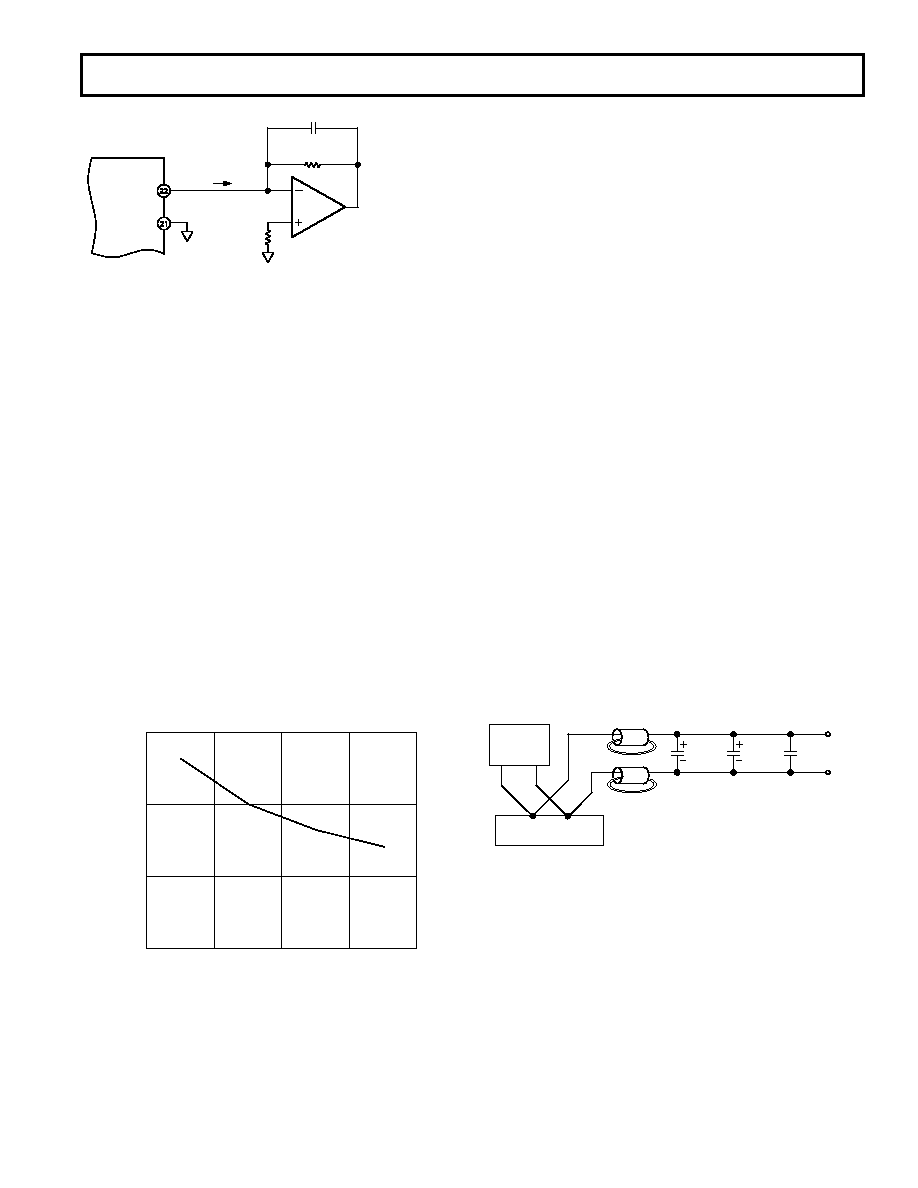
FREQUENCY – MHz
90
80
60
1.0
0.26
PSRR
–
dB
0.5
0.75
70
Figure 33. Power Supply Rejection Ratio of AD9752
Note that the units in Figure 33 are given in units of (amps out)/
(volts in). Noise on the analog power supply has the effect of
modulating the internal switches, and therefore the output
current. The voltage noise on the dc power, therefore, will be
added in a nonlinear manner to the desired IOUT. Due to the
relative different sizes of these switches, PSRR is very code depen-
dent. This can produce a mixing effect which can modulate low
frequency power supply noise to higher frequencies. Worst case
PSRR for either one of the differential DAC outputs will occur
when the full-scale current is directed towards that output. As a
result, the PSRR measurement in Figure 33 represents a worst
case condition in which the digital inputs remain static and the
full scale output current of 20 mA is directed to the DAC out-
put being measured.
An example serves to illustrate the effect of supply noise on the
analog supply. Suppose a switching regulator with a switching
frequency of 250 kHz produces 10 mV rms of noise and for
simplicity sake (i.e., ignore harmonics), all of this noise is con-
centrated at 250 kHz. To calculate how much of this undesired
noise will appear as current noise super imposed on the DAC’s
full-scale current, IOUTFS, one must determine the PSRR in dB
using Figure 33 at 250 kHz. To calculate the PSRR for a given
RLOAD, such that the units of PSRR are converted from A/V to
V/V, adjust the curve in Figure 33 by the scaling factor 20
× Log
(RLOAD). For instance, if RLOAD is 50 , the PSRR is reduced
by 34 dB (i.e., PSRR of the DAC at 1 MHz which is 74 dB in
Figure 33 becomes 40 dB VOUT/VIN).
Proper grounding and decoupling should be a primary objective
in any high speed, high resolution system. The AD9752 features
separate analog and digital supply and ground pins to optimize
the management of analog and digital ground currents in a
system. In general, AVDD, the analog supply, should be de-
coupled to ACOM, the analog common, as close to the chip as
physically possible. Similarly, DVDD, the digital supply, should
be decoupled to DCOM as close as physically as possible.
For those applications that require a single +5 V or +3 V supply
for both the analog and digital supply, a clean analog supply
may be generated using the circuit shown in Figure 34. The
circuit consists of a differential LC filter with separate power
supply and return lines. Lower noise can be attained using low
ESR type electrolytic and tantalum capacitors.
100 F
ELECT.
10-22 F
TANT.
0.1 F
CER.
TTL/CMOS
LOGIC
CIRCUITS
+5V OR +3V
POWER SUPPLY
FERRITE
BEADS
AVDD
ACOM
Figure 34. Differential LC Filter for Single +5 V or +3 V
Applications
Maintaining low noise on power supplies and ground is critical
to obtaining optimum results from the AD9752. If properly
implemented, ground planes can perform a host of functions on
high speed circuit boards: bypassing, shielding, current trans-
port, etc. In mixed signal design, the analog and digital portions
of the board should be distinct from each other, with the analog
ground plane confined to the areas covering the analog signal
traces, and the digital ground plane confined to areas covering
the digital interconnects.
All analog ground pins of the DAC, reference and other analog
components should be tied directly to the analog ground plane.
The two ground planes should be connected by a path 1/8
to 1/4 inch wide underneath or within 1/2 inch of the DAC to
相关PDF资料 |
PDF描述 |
|---|---|
| VE-2NM-MW-B1 | CONVERTER MOD DC/DC 10V 100W |
| VE-2NL-MW-B1 | CONVERTER MOD DC/DC 28V 100W |
| VE-2NK-MW-B1 | CONVERTER MOD DC/DC 40V 100W |
| AD9752ARZRL | IC DAC 12BIT 125MSPS 28SOIC |
| VI-J3R-MZ-B1 | CONVERTER MOD DC/DC 7.5V 25W |
相关代理商/技术参数 |
参数描述 |
|---|---|
| AD9752ARZ | 功能描述:IC DAC 12BIT 125MSPS 28-SOIC RoHS:是 类别:集成电路 (IC) >> 数据采集 - 数模转换器 系列:TxDAC® 产品培训模块:Lead (SnPb) Finish for COTS Obsolescence Mitigation Program 标准包装:50 系列:- 设置时间:4µs 位数:12 数据接口:串行 转换器数目:2 电压电源:单电源 功率耗散(最大):- 工作温度:-40°C ~ 85°C 安装类型:表面贴装 封装/外壳:8-TSSOP,8-MSOP(0.118",3.00mm 宽) 供应商设备封装:8-uMAX 包装:管件 输出数目和类型:2 电压,单极 采样率(每秒):* 产品目录页面:1398 (CN2011-ZH PDF) |
| AD9752ARZRL | 功能描述:IC DAC 12BIT 125MSPS 28SOIC RoHS:是 类别:集成电路 (IC) >> 数据采集 - 数模转换器 系列:TxDAC® 标准包装:47 系列:- 设置时间:2µs 位数:14 数据接口:并联 转换器数目:1 电压电源:单电源 功率耗散(最大):55µW 工作温度:-40°C ~ 85°C 安装类型:表面贴装 封装/外壳:28-SSOP(0.209",5.30mm 宽) 供应商设备封装:28-SSOP 包装:管件 输出数目和类型:1 电流,单极;1 电流,双极 采样率(每秒):* |
| AD9752-EB | 制造商:Analog Devices 功能描述:Evaluation Board For AD9752 制造商:Analog Devices 功能描述:DEV TOOLS, EVAL BD FOR AD9752 - Bulk |
| AD9752-EBZ | 功能描述:BOARD EVAL FOR AD9752 RoHS:是 类别:编程器,开发系统 >> 评估板 - 数模转换器 (DAC) 系列:TxDAC® 产品培训模块:Lead (SnPb) Finish for COTS Obsolescence Mitigation Program 标准包装:1 系列:- DAC 的数量:4 位数:12 采样率(每秒):- 数据接口:串行,SPI? 设置时间:3µs DAC 型:电流/电压 工作温度:-40°C ~ 85°C 已供物品:板 已用 IC / 零件:MAX5581 |
| AD9753 | 制造商:AD 制造商全称:Analog Devices 功能描述:Analog Devices: Data Converters: DAC 12-Bit, 10 ns to 100 ns Converters Selection Table |
发布紧急采购,3分钟左右您将得到回复。